
Jessica Rowbury speaks to Marie Semeria, CEO of Leti, about how the organisation has supported technology innovation throughout its 50-year history
This year, global technology research institute Leti is celebrating 50 years of innovation. Founded in 1967 as a research division of the French Atomic Energy Commission (CEA), Leti has evolved into a global leader in micro- and nanotechnologies, serving as a bridge between basic research and production of innovative miniaturisation solutions.
To mark its 50th anniversary, Leti has organised special events throughout 2017 at its headquarters in Grenoble, France, and at major industry events such as Semicon West and IEDM. Its most recent occasion, Leti Innovation Days, featured a conference discussing how microelectronics is helping address environmental and healthcare challenges, in addition to an exhibition with new product demonstrations and a startup area. The event took place on 28-29 June in Grenoble.
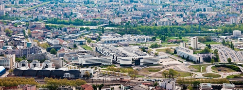
Let's headquarters are in Grenoble, France
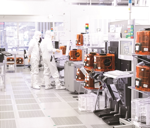
Leti solutions target a wide variety of sectors, including sustainable transport systems, telecommunications, health, consumer electronics, energy, smart cities, defence and security and space. Its 8,500m² of cleanroom space features 200mm and 300mm wafer processing of micro and nano solutions for applications ranging from space to smart devices.
Although Leti was formed primarily as a microelectronics centre, photonics has been paramount to much of its research and product development, according to CEO Marie Semeria. ‘Leti’s DNA is in electronics and photonics,’ she said.
Recent successes in the photonics domain include the demonstration of the world’s first wide video graphic array (WVGA) GaN microdisplay with 10-micron pixel pitch, designed for augmented reality applications, and the co-integration of an indium phosphide (InP) laser on a photonics circuit on silicon.
A sure start
To help ensure that these types of innovative technologies reach industry, Leti partners with a range of companies, ranging from large industrials to SMEs and startups.
Since its founding, the organisation has launched 60 startups in a range of industries, for example virtual reality firm Motion Recall, fluorescence imaging company Fluoptics, and even companies that have gone on to become huge global entities, such as STMicroelectronics.
Over the last 50 years, new photonics companies in France have benefitted from an environment that favours start up creation, according to Semeria, in addition to close collaboration with the research sector, which is made up of more than 141 active laboratories.
‘French academic institutes and technological research organisations create and sustain start-ups in the photonics domain,’ she said.
Startups make up a large part of the photonics industry in France – 49 per cent of the companies employ less than 20 people and achieve four per cent of the turnover. Moreover, 40 per cent of the large industrial photonics players were formed less than 10 years ago.
In addition to France, there are high numbers of photonics startups emerging across Europe, Semeria noted, which in part is thanks to the European Union recognising photonics as key enabling technology (KET), which has helped drive funding initiatives on both a European and national level, Semeria noted.
Another factor contributing to there being high numbers of startups in photonics is the richness of the domain and its ability to fulfil a large variety of needs and use-cases. This opens the way to niche applications where companies can become leaders, Semeria said, pointing to Teem Photonics, Imagine Optic, Keopsys and eLichens, which are specialists in laser sources, wavefront analysers, fibre laser sources and NDIR gas sensors, respectively.
Having such a large number of micro-niches also allows for the emergence of small companies that can play a worldwide role, Semeria added.
In order to continue to foster innovation in France and in Europe, it will important to launch companies that can keep their production in the region while still remaining competitive, Semeria explained, pointing to the Sofradir group and STMicroelectronics as successful examples of this.
The next 50 years of innovation
With photonics being a relatively new industry, it opens the way to various potential non-explored applications. Newer applications areas such as augmented reality, wearables, autonomous driving, and quantum communications and computing are where Semeria believes photonics will enable major innovations and technological breakthroughs in the future. However, as well as these emerging markets, innovation will also still be essential in traditional sectors like security, telecoms, healthcare, and automotive.
Going forwards, integration between the III-V world and silicon world will be crucial to foster the development of new functions, Semeria said. For example, the heterogeneous integration of microelectronics and photonics on the same chips, such as photonics on silicon.
Innovation in this area will be assisted through Let’s involvement with the III-V Lab in France, a private R&D organisation jointly established by Nokia, Thales and the CEA. II-V lab offers pre-commercial and customised production of III-V components or epitaxy wafers for leading edge innovative products. ‘The rationale of this cooperation is based on the mix of photonics on silicon and III-V materials,’ Semeria noted.
