Ivan Nikitski, EPIC’s Photonics Technology Program Manager, talks to Jan Trommershausen, Managing Director of AEMtec, a Berlin-based manufacturer of complex micro- and optoelectronic modules and systems.
What’s the background to your appointment as MD at AEMtec?
In 1990, after studying physics and finance at the University of Muenster, I worked in the planning department of a company that offered maintenance on power plants and refineries. In 1998, I moved to DBT Deutsche Bergbau-Technik, a company involved in mining and heavy engineering, where I worked as head controller. Three years later, I was offered the job of MD at DBT Maschinenfabrik Scharf, a subsidiary making underground transportation for equipment and people for mines. I was involved in restructuring, which was tough and challenging. In 2001, I became CEO at SaarGummi, and in 2006, I worked as CFO for exceet Card Group AG. In 2009, I was offered the position of MD at AEMtec, a Berlin-based spin-off from Infineon Fiber Optics, specialising in unpackaged semiconductors for the data and telecoms market. The company was experiencing difficulties and the owners gave me three months to decide whether it could be turned around or should be put up for sale.
How has AEMtec developed since then?
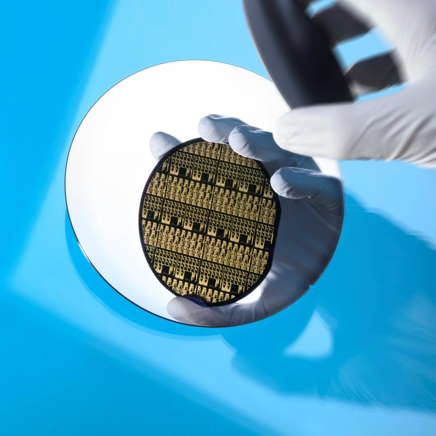
In the beginning, we worked almost exclusively in data communication, with Infineon as our biggest customer. But since then, we have reinvented the company by going into new markets and moving into the development, industrialisation and manufacture of complex micro- and optoelectronic modules and systems. Our first step was to collaborate with medtech customers, especially in digital imaging, for example, detector modules for CT scanners. This required acquiring ISO certification for medical devices. Later on, we were able to apply this knowledge to components for the semiconductor industry. Over the past 13 years, we’ve grown from 68 employees to just over 230, and over the same period, our annual turnover has increased from €13m to around €70m.
What are your main products and application fields?
We focus on miniaturised electronics for our customers’ core components, operating within a low volume/high mix niche. We can offer a wide range of assembly and packaging solutions that we call customised advanced packaging. Around 35% of our revenues are from German customers and 55% from Europe. The rest is mostly the US, which is a growing market for us. We have one small subsidiary in Boston, with an engineer and sales team.
We’ve been involved in more than 500 projects, and the experience we have gained comprises our background IP. Customers come to us with their ideas for projects or prototypes and we industrialise them so that the components can be produced in comparatively low volumes here in Berlin. Minimum volume is around 100 pieces a year and the maximum is about 500,000 sensors a year for certain applications.
We have a strong background in digital imaging. Electronics and optics are becoming more and more integrated, and we are in the middle of this trend. We try to identify new technologies which are feasible for a certain industrialised production process, not only on a lab basis but also for serial production.
We work in a wide variety of application fields including medical technology, data & telecoms, industry & automation, semiconductors and automotive & transport. A growing market for us is aviation & aerospace as well as industrial applications like 3D cameras and gas sensors.
What are the technological challenges in this process?
Precision is one. Products are getting smaller and smaller, which can be a challenge for our high-precision placement equipment. Placement accuracy is always driven by the quality of the cameras inside because we don’t only look at the corner of a chip, we look to the active area of the chip to place in a way it needs to be placed and today we are down to maybe half a micron in placement accuracy.
Another issue is cleanliness, particularly with the cameras. We have clean rooms starting with ISO8 down to ISO5, which is semiconductor level. We are currently working on residual gas analysis, for example, where we have to ensure that the semiconductor piece of equipment is supported by this kind of cleanliness level.
How do you see the future?
One of the trends coming in Europe and that’s already strong in the US is a lot of complex development and manufacturing processes are being pulled back to Europe and the US from Asia. Of course, the chips will be more expensive than those produced in Taiwan, but there is a logic behind it and it is likely to continue. Climate change is another challenge, and we were CO2-neutral the end of 2022. The power we buy is now all from natural resources and we don’t have to buy gas because we use the heat from our soldering machines to keep the factory warm. The third challenge is the shortage of talent. The number of electronics companies in the Berlin area is growing, so we are working with other companies and the employment agency here in Berlin to organise special training on micro-technologies.
What can be done to make the European photonics industry more competitive?
The European photonics industry has got a great future, but there is always room for improvement. One way would be to adopt the US approach, which is a continuous process of trial and error: if something doesn’t work, they scrap it and try something else. In Europe, we like to avoid risks and think more long-term. We’re also much more regulated than the US, which can lengthen time to market.
If you started again, what would you do differently?
Although I enjoy my work and I’m still highly motivated, if I started again, I’d probably become a carpenter and produce furniture. I love the look and smell of wood and the way it grows.
What’s your advice for the next generation of entrepreneurs?
As a customer once told me, make sure you know where you’re going and make sure that everybody is on the same track. Secondly, collect experiences and keep learning. This means not having a 9 to 5 mentality and volunteering to do complicated or difficult tasks that nobody else wants to do. Finally, enjoy what you do and invest time in your own happiness and in your own motivation. You will get it all back in the positive feedback from customers and employees.