Skip to main content
Social media links EO
LinkedIn
Twitter
Log in
Register
Applications
Life sciences
Environment
Quantum
Defence
Automotive
Aerospace
Medical engineering
Electronics
Optical communication
Technologies
Illumination & energy
Imaging
Industrial lasers
Lasers & optoelectronics
Sensors, test & measurement
Photonics 100
UK Photonics
Photonics Frontiers
Resources
Webcasts
White Papers
Supplier
Events
Products
Search
Polarised Raman Spectroscopy
Electroluminescence and Photoluminescence Spectroscopy of a Phosphorescent Organic Light Emitting Diode (PhOLED)
Time-Resolved Electroluminescence Spectroscopy of a White Light Emitting Diode
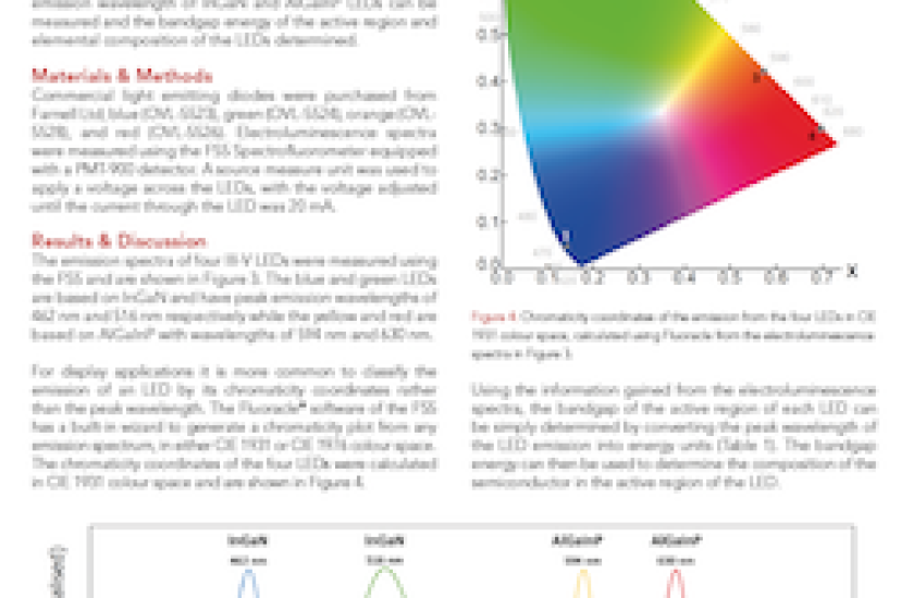
Determination of Chromaticity Coordinates and Bandgaps of III-V LEDs Using Electroluminescence Spectroscopy
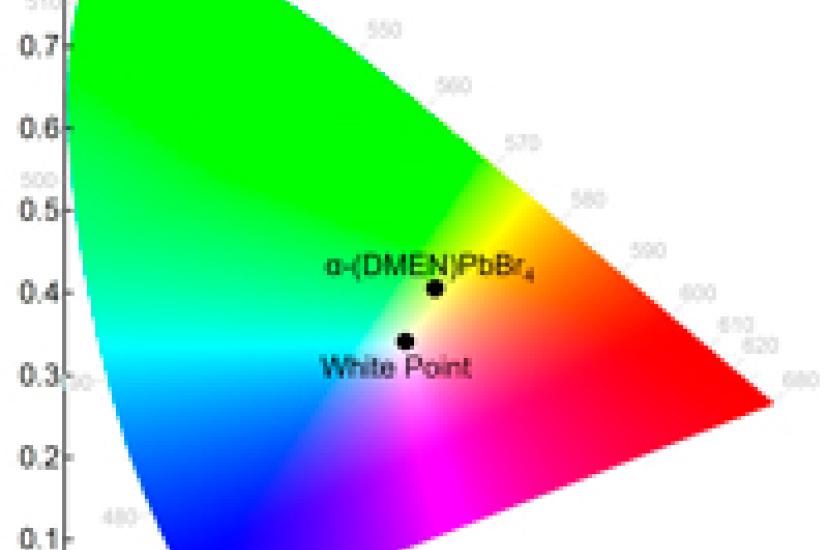
Photoluminescence Spectroscopy of a White-Light Emitting Perovskite
Excitation-emission spectroscopy with charge coupled detectors
Media Partners