Moore’s Law came into being more than 50 years ago, when a research specialist at American semiconductor company, Fairchild Semiconductor, suggested that the number of transistors in dense integrated circuits could double every two years.
That specialist, Gordon Moore, consequently predicted that the speed and capability of computers would also increase every two years. Moore’s prediction has since been used in the semiconductor world for planning and product development, and has been a near-reality ever since. This has been driven by advances in photolithography, one of the key technologies behind size reduction of computer chip components.
While there is not a definitive consensus about when, or if, Moore’s law will come to an end, there has been speculation that semiconductor advancement has slowed in the past 10 years. However, in the last two years, manufacturers of this technology have developed new, mass-fabrication practices, for which lasers play a crucial role.
Some recent market predictions appear to dispute the slowing of semiconductor development altogether. The Semiconductor Industry Association recently announced that global sales of semiconductors totalled $113.6bn in the third quarter, an increase of 11 per cent on the previous and a 5.8 per cent increase year-on-year. Looking ahead, Technavio’s Global Semiconductor Market 2020-2024 report forecasts that the global market size will grow more than $90bn by 2024.
Driven by 5G
Technavio’s report states that major market growth came from the integrated circuits segment last year, which is expected to experience the fastest growth during the next five years, largely because of the growing investments in telecommunication network deployments, including 5G networks.
The most recent, and arguably one of the most famous, examples is the iPhone 12. The new smartphone features what Apple calls the world’s first processor built from 5nm transistors: the A14. The processor was supplied to Apple by Taiwan Semiconductor Manufacturing Company (TSMC), for use in its smartphones, tablets and Mac computers. It is anticipated that the transistors – which are about the width of 25 atoms – will also begin to appear in some of the leading PCs, servers and smartphones from multiple vendors in the next year.
To put the size of the transistors into context – and return to Moore’s Law – there are about 171 million of them laid out over every square millimetre of the chip. This has been possible thanks in no small part to Dutch firm ASML.
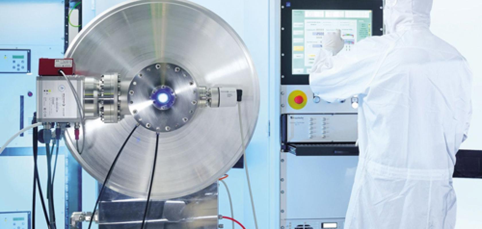
The lithography system manufacturer developed a technique to carve circuitry patterns into silicon via extreme ultraviolet (EUV) lithography – and this is where lasers earn their stripes. Back in 2018, laser manufacturer Trumpf described at Epic’s Executive Meeting on Industrial Lasers how it was using CO2 lasers to develop EUV lithography systems for this purpose. Dr Andeas Popp, a project head at Trumpf Photonic Components, explained that this new application of CO2 lasers will be key for taking the next step in Moore’s law. This is because the size of semiconductor structures on chips are approaching atomic dimensions – something that has been made possible by complex exposure processes enabled by lasers.
To the limit
Previously, exposure processes had been performed using UV radiation generated by 193nm excimer lasers. But this wavelength range faces limitations when producing structures less than 10nm in size. For structures in the range of 5nm, exposure at shorter wavelengths in the EUV range must be used to provide the resolution necessary for their fabrication.
Trumpf collaborated with ASML, its subsidiary Cymer and optics giant Zeiss, to develop the systems. The EUV lithography technology quickly generated interest from major semiconductor manufacturers, according to the company, with such end-users placing orders for the systems, to ramp up their mass production throughout 2018 and 2019.
TSMC was one such company, and is now sole supplier of the A14 processor to Apple. Samsung is also putting the technology to good use, and is set, alongside Qualcomm, to imminently reveal a new processor for Android phones. Then there is Intel, which is reportedly looking to start using the technology next year.
Counteracting the cost
But what about start-up companies, or those of a smaller or medium size (SMEs)? The ASML machines cost in excess of $120m (£90m) each, which is high even compared with other semiconductor industry tools.
This has led many speculators to argue that, because the cost of a single EUV layer on a chip is about three times the cost of a layer that uses traditional processing, this cancels out the benefits of transistors this size.
Moreover, Moore’s Law historically yielded 40 per cent reductions in transistor cost, but the benefit from this new technology will be closer to around 10 per cent. In addition, by prohibiting smaller businesses and start-ups from accessing the technology, the cost could also prevent more new and exciting developments reaching the market.
To help counteract this problem, Fraunhofer ILT is developing technologies for the production of nanostructures that start-ups or SMEs can also afford. The idea, revealed Dr Serhiy Danylyuk, team leader of EUV and DUV technology at the institute, is to generate periodic structures via the interference effects of coherent radiation, like the achromatic Talbot effect. In the near field – less than 500µm behind a mask – an intensity distribution is created with which microlithographic structures can be produced.
Danylyuk explained: ‘The cost of the systems is exorbitant right now and it is not going to become cheaper any day soon. So, we got thinking that we could try to scale down and make it possible for SMEs.’
Scientists at the institute are doing this using a KrF excimer laser at a wavelength of 248nm to generate structures with a period of several hundred nanometres. This was tested with a Leap150K laser system from Coherent. In a photoresist, 180nm wide lines can be generated with a period of 600nm. With higher energies of 250mJ/cm², silicon on glass can also be ablated with similar dimensions. The technology is also well suited for the ablation of PET plastic surfaces on a 300nm scale.
The principle also works with wavelengths in the EUV, as used to produce the 5nm transistors. The institute developed its own beam source for this purpose, the FS5440. This is based on a gas discharge, and can generate the required radiation at 13.5nm wavelength. It is also much more compact than the laser-based EUV source used in large-scale industrial facilities.
‘There are three main cost factors in EUV technology,’ continued Danylyuk, ‘the point of source; the optical system, which is extremely expensive and technologically advanced in the large scale; and, of course, the positioning system, which places high demands in the nanometre range. We thought that smaller laser sources would be the best thing. We are basically happy to use any kind of source, depending on customer requirements, but we believe our own plasma source to be the cheapest.’
Masks or mirrors?
Transmission masks were used as an alternative optical scheme to reduce the amount of mirrors required in the system.
‘We worked on a simpler scheme, using transmission masks not as expensive as mirrors,’ said Danylyuk. ‘We developed these in-house and it means we can use maybe one or two mirrors in the system, not nine. This is not necessarily as scalable as using reflective masks, but if you are an SME going for smaller volumes, this approach could work. The mask is positioned in the vicinity of the wafer, and we can demagnify the structure by a factor of two.’
In terms of cost, while Danylyuk acknowledged that, while it may never reach the thousand-dollar mark, the system under development will still be significantly more accessible than those currently available. ‘I think we will be looking at low six numbers,’ he said. ‘It depends on the requirements on the source side.’
Discussing the challenges of working toward such a technology – which has been in development at Fraunhofer ILT for almost 10 years – Danylyuk said: ‘It’s probably hard to go to the resolution of 5nm and below with this technology, but we are looking at a sub-20nm scale already, and whether SMEs need such a small resolution. It should be scalable to 10nm but it’s challenging, both from a mass-manufacturing and a positioning point of view. Systems have to become more expensive if you want to drive to single nanometre precision. Somewhere we need to make a cut and say “that’s perhaps not what SMEs would need anyway”.’
An additional challenge for the institute came with the positioning of the mask. ‘We had to position it in a sub-millimetre distance to the wafer, and make sure that the distance is maintained over the full wafer size,’ said Danylyuk. ‘So we developed a technology for maintaining dynamic distance. Our system is currently working with 100mm wafers, and there is no reason why it cannot go larger, but the medium size is what many of the SMEs are comfortable with, and there is a lot of technology available for this wafer size.’
Ready and waiting
So, how do SMEs get their hands on this technology? ‘Everyone is welcome to use our facility to test this technology,’ said Danylyuk. ‘Depending on the end-use, we can also speak with our partners about how to bring the technology to the market. This way, people can get an idea of whether it is suitable for them, and what kind of effort is needed to bring it into their facility.’
It is also worth noting if, after taking these steps, SMEs still feel that the technology is out of their reach, there are other options available. ‘If the cost is still too high, they could consider using far ultraviolet (FUV) as the laser source,’ said Danylyuk. ‘It uses a similar technology and the same type of approach that we use in EUV, but with FUV – and this may not give you the sub-10nm structures, rather 100 to 150nm – the technology is more scalable by using commercially available UV laser sources.
‘So, for people who may only need to use structures on the scale of under 200nm, with different materials, we can offer the development of lithography-based UV, and also direct laser structuring technology.’
