A team of researchers from the California Institute of Technology (Caltech) has developed a tiny silicon chip that uses ‘light bending’ technology to project illuminated images, led by Professor Ali Hajimiri. Only one square millimetre in size, the chip can turn a smart phone into a projector without the need for bulky and expensive bulbs and lenses. The research was presented at the Optical Fiber Communication (OFC) conference in San Francisco on 10 March.
Traditional projectors — like those used to project a film or classroom lecture notes — pass a beam of light through a tiny image, using lenses to map each point of the small picture to corresponding, yet expanded, points on a large screen.
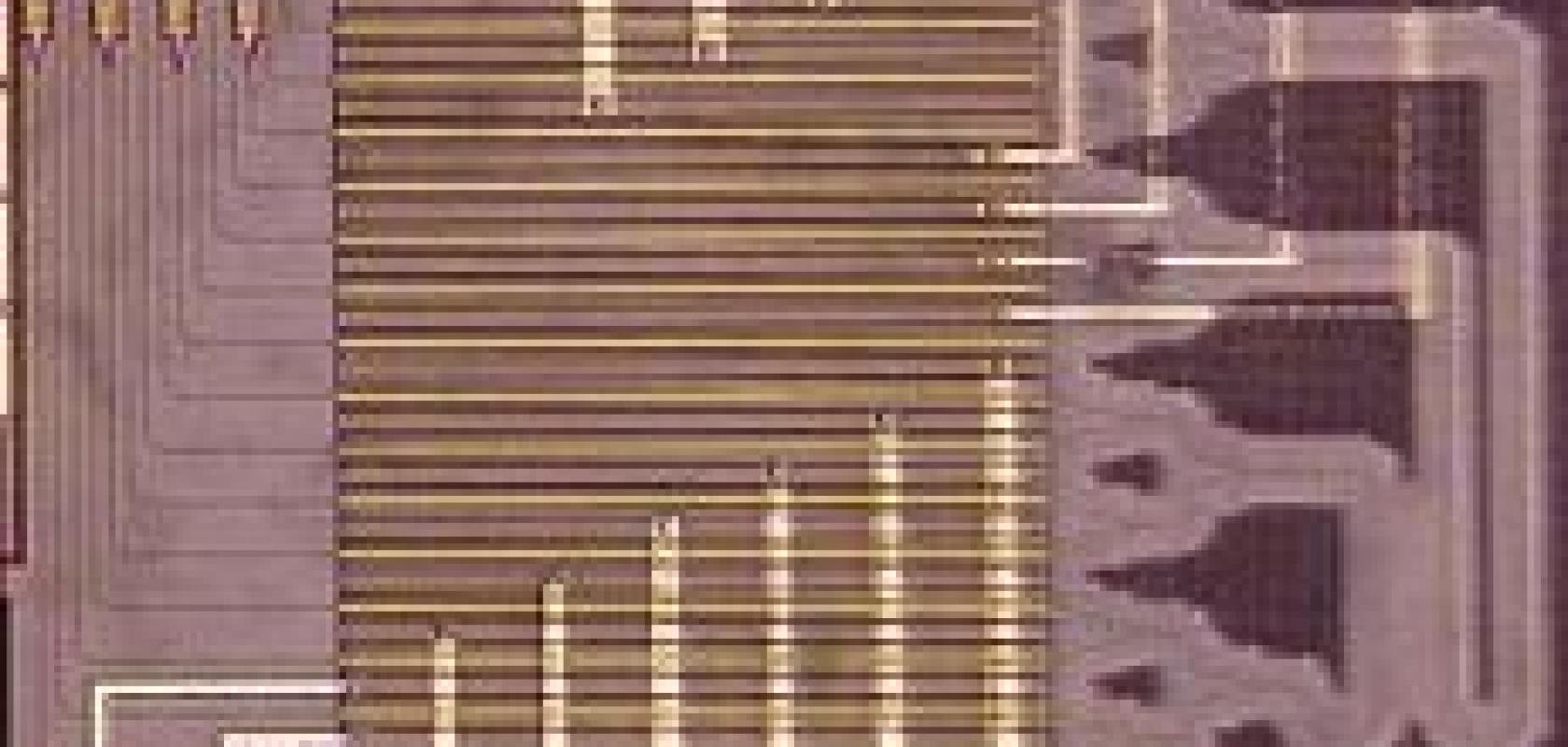
The Caltech chip eliminates the need for bulky and expensive lenses and bulbs and instead uses an integrated optical phased array (OPA) to project the image electronically, with only a single laser diode as light source and no mechanically moving parts.
The researchers were able to bypass traditional optics by manipulating the coherence of light. If two waves are coherent in the direction of propagation, the waves combine, resulting in one wave and a beam with twice the amplitude and four times the energy as the initial wave, moving in the direction of the coherent waves.
‘By changing the relative timing of the waves, you can change the direction of the light beam,’ said Hajimiri. ‘For example, if 10 people kneeling in line by a swimming pool slap the water at the exact same instant, they will make one big wave that travels directly away from them. But if the 10 separate slaps are staggered — each person hitting the water a half a second after the last—there will still be one big wave, but with the wave bending to travel at an angle.’ Using a series of phase shifters, the OPA chip similarly slows down or speeds up the timing of the waves, thus controlling the direction of the light beam.
To form an image, electronic data from a computer are converted into multiple electrical currents. By applying stronger or weaker currents to the light within the phase shifter, the number of electrons within each light path changes — which, in turn, changes the timing of the light wave in that path. The timed light waves are then delivered to tiny array elements within a grid on the chip. Then, the light is projected from each array in the grid and the individual array beams combine in the air to form a single light beam and a spot on the screen.
As the electronic signal rapidly steers the beam left, right, up, and down, the light acts as a very fast pen, drawing an image made of light on the projection surface. Since the light draws many times per second, the eye sees the process as a single image.
So far, the images the team can project with the current version of the chip are simple, such as a triangle, a smiley face, or single letters. However, the researchers are currently experimenting with larger chips that include more light-delivering array elements that can improve the resolution and increase the complexity of the projected images.
In their recent experiments, Hajimiri and his colleagues have used the silicon chip to project images in infrared light, but additional work with different types of semiconductors will also allow the researchers to expand the tiny projector's capabilities into the visible spectrum. ‘Right now we are using silicon technology, which works better with infrared light. If you want to project visible light, you can take the exact same architecture and do it in what's called compound semiconductor III-V technology,’ explained Firooz Aflatouni, a co-author on the paper and assistant professor at the University of Pennsylvania. ‘Silicon is good because it can be easily integrated into electronics, but these other compound semiconductors could be used to do the same thing.’
‘In the future, this can be incorporated into a phone, and since there is no need for a lens, you can have a phone that acts as a projector all by itself,’ Hajimiri added. However, he pointed out that a tiny projection device could have many applications, including light-based radar systems (LIDAR), which are used in positioning, robotics, geographical measurements, and mapmaking. Existing LIDAR technology requires complex, bulky, and expensive equipment, which could be simplified to a single chip at a much lower cost. ‘The beauty of this thing is that these chips are small and can be made at a very low cost — and this opens up lots of interesting possibilities,’ he added.
