Scientists at the Technische Universität München (TUM) have demonstrated laser action in semiconductor nanowires, which could potentially speed up computing, as well as having applications in communications and sensing.
The thread-like semiconductor structures, called nanowires, are so thin that they are effectively one-dimensional. The nanowires developed by the researchers emit light at technologically useful wavelengths and operate at room temperature. They now have documented this breakthrough in the journal Nature Communications and, in Nano Letters, have disclosed further results showing enhanced optical and electronic performance.
‘Nanowire lasers could represent the next step in the development of smaller, faster, more energy-efficient sources of light,’ said Professor Jonathan Finley, director of TUM's Walter Schottky Institute.
Potential applications include on-chip optical interconnects or even optical transistors to speed up computers, integrated optoelectronics for fibre-optic communications, and laser arrays with steerable beams. Nanowires are also highly sensitive to their surroundings, explained Finley. They have a large surface-to-volume ratio and are small enough, for example, to be inserted into a biological cell, making the lasers useful in environmental and biological sensing.
These experimental nanowire lasers emit light in the near-infrared, which is ideal for fibre-optic communications. They can be grown directly on silicon, presenting opportunities for integrated photonics and optoelectronics. And they operate at room temperature, a prerequisite for real-world applications.
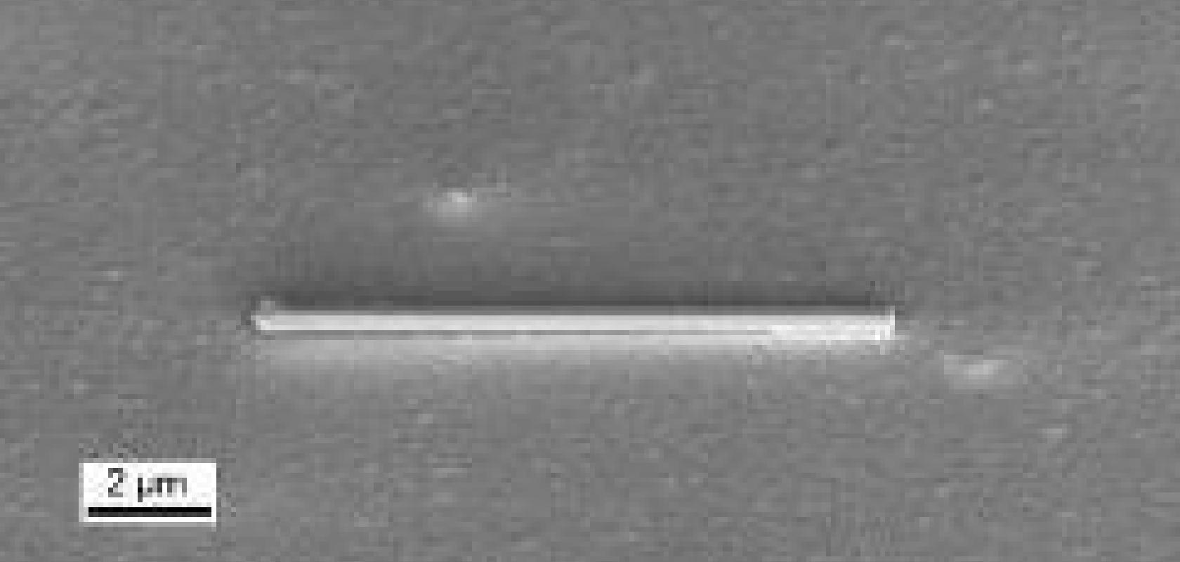
The nanowire lasers demonstrated at TUM have a complex core-shell cross-section with a profile of differing semiconductor materials tailored virtually atom by atom.
The nanowires' tailored core-shell structure enables them to act both as lasers, generating coherent pulses of light, and as waveguides, similar to optical fibres. Like conventional communication lasers, these nanowires are made of III-V semiconductors, materials with the right bandgap to emit light in the near-infrared.
A unique advantage, Finley explained, is that the nanowire geometry is ‘more forgiving than bulk crystals or films, allowing you to combine materials that you normally can't combine’.
Because the nanowires arise from a base only tens to hundreds of nanometres in diameter, they can be grown directly on silicon chips in a way that alleviates restrictions due to crystal lattice mismatch – thus yielding high-quality material with the potential for high performance.
‘At present, very few labs in the world have the capability to grow nanowire materials and devices with the precision required,’ said co-author Professor Gerhard Abstreiter, founder of the Walter Schottky Institute and director of the TUM Institute for Advanced Study. ‘And yet, our processes and designs are compatible with industrial production methods for computing and communications.’
