Silicon photonics has evolved over the past 30 years, from the comparatively simple interconnects of the late 1980s to the more advanced devices available today. The advantages are clear; the ability to carry more data in less time, using less energy than electrical conductors, is invaluable to manufacturers who are trying to meet today’s insatiable demand for instant and unlimited data from ever-smaller devices. However, the manufacture of silicon photonic devices is costly, and wafer probing prior to packaging – and testing during packaging – is essential to ensure product quality. Scott Jordan, Head of Photonics at Physik Instrumente, discusses this evolving technology and describes how advances in precise nanoscale alignment are significantly cutting time and costs associated with the manufacturing process.
Our insatiable desire for data – supercomputers in our pockets, streaming media, cloud computing and the internet of things – means that the need to carry more data in less time has never been greater. The United States currently consumes more electricity running its data centres than it does on lighting, and there are no signs that the rate of increase in demand is slowing.
Interconnects – the connections between devices – currently represent the major bottleneck for data speed and bandwidth, and this is where the bulk of computing energy is expended. Moving from conventional electrical conductors to photonic interconnects is helping to address these issues.
A chequered past
The history of the photonics industry has been one of continuously diminishing scales. The industry was brought to life by large scale projects around 1997 – the start of the boom years – when satellite links for telecommunications were being replaced by transoceanic, transcontinental and regional fibres. But how many transatlantic cables do you really need? The next step was bringing fibre to every home, which not only required a reduction in the scale of photonic interconnects, but also called for a huge increase in production to meet the growing demand. Unfortunately, this rapidly growing market for photonics led to an over-confidence in the industry, and in 2002 it collapsed almost overnight – like flipping a switch.
Despite this, the idea of developing photonic devices on an ever-diminishing scale wasn’t forgotten, and R&D in this area continued quietly. Forward thinking engineers realised that the growing need for data handling and storage would require components that could connect data centres, racks within data centres, boxes within racks, cards within boxes and chips within cards, and that with each reduction in scale the potential market would increase.
Fast forward a decade and a half, and we are now pushing the boundaries of this approach – creating the smallest possible interconnects – and this has seen the industry begin to move away from conventional electrical conductors to photonic interconnects, to the point where photonic devices are incorporated onto chips alongside the conventional microelectronics. Broadly speaking, the initial design and materials challenges associated with manufacturing silicon photonics have now been met, but the industry is still struggling with the practicalities of testing and packaging these complex components.
Not as easy as it looks
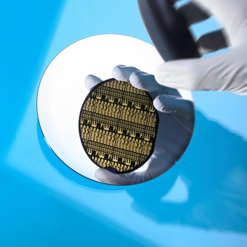
With all microelectronics, you have to evaluate every single device while it’s still on the wafer to make sure that it is operating correctly, a process known as ‘probing the wafer’. For conventional microelectronics, you bring electrical probes into contact with the devices, then light them up to determine if they are alive and to assess their quality. This is to avoid the significant downstream costs associated with the packaging process – where wires and fibres are attached and everything is put together – for faulty components. Manufacturers therefore need to determine with great accuracy and reliability whether devices are working correctly before the wafer goes any further.
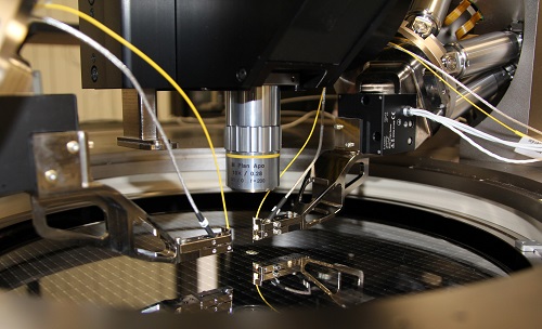
If you add photonic devices into the mix, then you can no longer just take an electrical probe and make contact, you also have to couple light into and out of the device while it’s still on the wafer. This was not an issue 20 years ago – or even five – but with the latest generation of silicon photonics, there could be thousands of devices on a wafer, all needing optical probing. This requires test rigs that can accurately align to within tens of nanometres and to effectively assess numerous parallel optical paths with interacting inputs and outputs. The issue is compounded by the need for rapid alignment and absolutely no unwanted contact with the wafer. These challenges are all reproduced at multiple points in the production chain, including during packaging, when the devices need to be re-checked to ensure that everything is still working and that all devices still meet the manufacturing specifications.
This is an area of the photonics industry that is currently greatly underserved and, as such, the market for probing and packaging in silicon photonics is about to explode. Companies like Physik Instrumente, as well as many of its customers, are laying the groundwork for this forthcoming revolution, and are actively engaged in tackling the challenges of precision automation for the purposes of probing and packaging in the photonics industry. For example, its recent introduction, the Fast Multichannel Photonics Alignment (FMPA) engine, uses a fully parallel gradient search to align multiple couplings, multiple degrees of freedom, and multiple channels, even if they interact.
The key advantage of this unique approach is that it achieves all of these adjustments in a single step with a simple set of commands, compared to previous set-ups where the couplings had to be optimised in a sequential fashion, constantly going back and forth and readjusting at each stage to gradually reach a consensus. This took a considerable amount of time, which of course had a significant impact on price, overall efficiency and scalability in the face of skyrocketing demand.
In contrast, the FMPA engine can do in a few seconds what once took hours. It’s no surprise then that the system has already been recognised by several industry bodies, and is going to appear on the radar for many, whether they are making the wafers, the packaging apparatus, or the tooling that performs the testing and the packaging. At the moment, everyone is chasing production economics, and being able to reduce alignment times by two to three orders of magnitude, is a huge advantage.
And then what?
This is by no means the end of the silicon photonics story though. The next step after resolving the connectivity infrastructure challenges is optical computing – where the logic itself is performed optically – and this is likely to be followed by quantum computing, which is approaching faster than anyone would have thought. Both of these research areas will have a significant photonics aspect, so it’s really just the beginning. In terms of probing and packaging, what’s next is more of the same: greater speed, smaller sizes and more embeddable configurations that can be easily slotted into equipment.