As Ayar Labs secures investment to develop its silicon photonics technology, Robert Roe speaks to Hugo Saleh about the firm's plans
A partnership between HPE and Ayar Labs aims to develop silicon photonics solutions that will support the next generation of advanced computing systems.
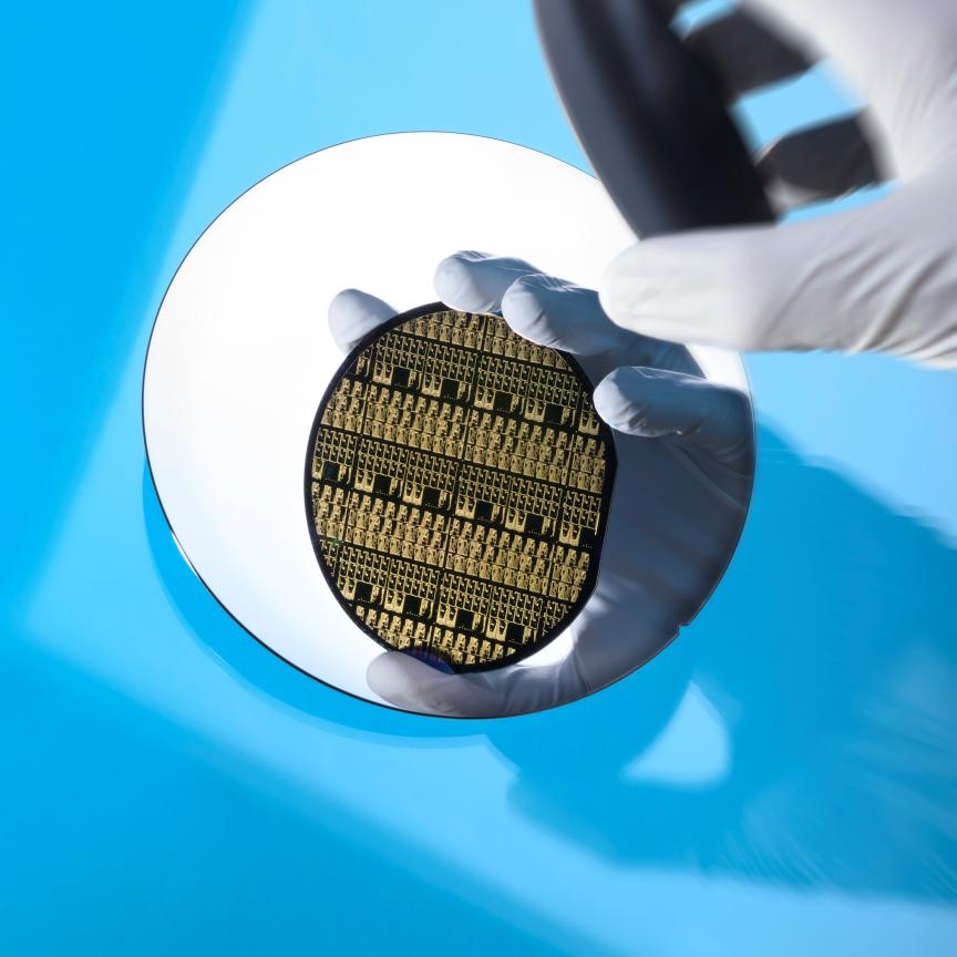
Hewlett Packard Enterprise and Ayar Labs recently signed a multi-year strategic collaboration to accelerate the networking performance of computing systems and data centres by developing silicon photonics solutions based on optical I/O technology.
Silicon photonics will be used to enhance the networking capabilities and support future requirements for high performance computing (HPC), artificial intelligence, and cloud computing architectures. The technology also has the potential to reduce the amount of energy used in data centres and large computing systems.
The two organisations also announced that HPE’s venture arm, Hewlett Packard Pathfinder, has made a strategic investment in Ayar Labs to accelerate the development and adoption of joint future technologies.
Hugo Saleh, Ayar Labs senior vice president of commercial operations, stated: ‘Within the press release, we talked about a few things. One is a future design of HPE Slingshot architecture, which has its genesis back at Cray. Today it is their high-end, Ethernet-like, networking solution that is targeted for HPC. We're also working with HPE on advanced architectures where we're talking about the composability of disaggregated resources, with an intelligent software stack.’
This investment demonstrates HPE’s commitment to silicon photonics as a way to overcome the challenges of solving the memory bottleneck for future high-performance computing systems, such as those found in HPC and AI. The added benefit of using silicon photonics technologies is the potential to use the high-bandwidth networking capabilities of optical I/O to support the development of disaggregated computing architectures.
Photonics underpins next-generation computing
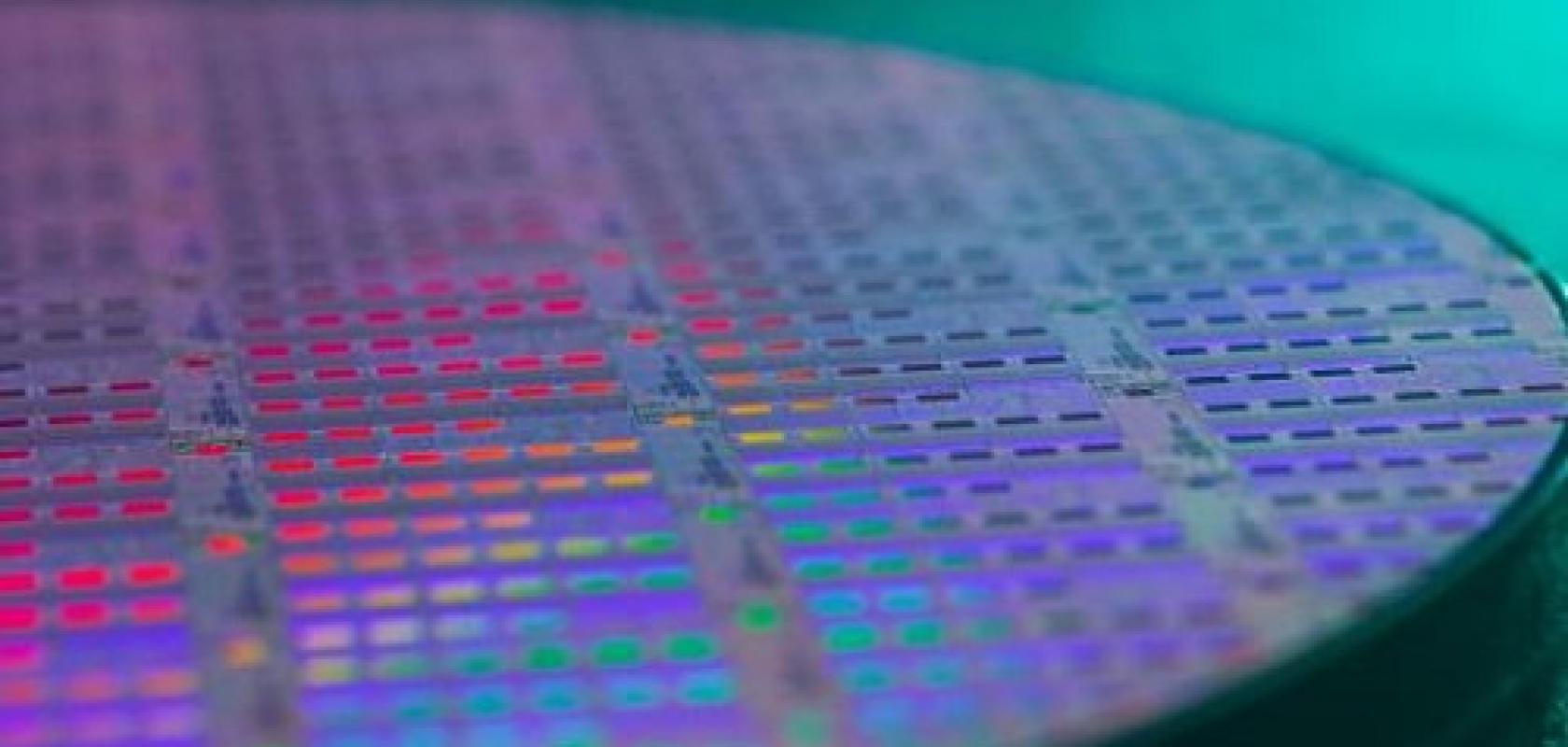
Ayar Labs' current technology consists of the optical I/O chiplet, TeraPHY, and a light source called SuperNova. The light source provides up to 16 wavelengths of light, powering up to 16 ports. SuperNova is a multi-wavelength, multi-port, remote light source with 64 wavelengths for advanced integrated optics applications, including AI, optical computing, and optical I/O wave division multiplexing (WDM). The optical source is compliant with the CW-WDM MSA 400 GHz wavelength grid and operates uncooled from 15 to 100°C.
The multi-wavelength source consists of a single frequency, distributed feedback (DFB) laser array coupled to a laser distribution network. Together, the laser and distribution network generates eight wavelengths across eight fibres, for a total of 64 addressable wavelength carriers.
This technology could massively increase the memory bandwidth for future HPC and AI systems, as each chiplet delivers the equivalent of 64 PCIe Gen 5 lanes, which provides up to two terabits per second of I/O performance. The system uses standard silicon fabrication techniques along with disaggregated multi-wavelength lasers to achieve high-speed, high-density chip-to-chip communication with power consumption at a picojoule range.
‘There are two reasons why you'd want to disaggregate the laser first,’ Saleh noted. ‘The SoC tends to be a very hostile environment; [it's] very common for these high-power CPUs to get to 125-plus degrees Celsius.'
While the silicon is qualified to run at those temperatures, Saleh explained, lasers are susceptible to problems from temperature changes. ‘High temperature causes early degradation and when the temperature moves up and down, your light actually shifts in frequency.’
Ayar Labs developed its technology alongside Global Foundries as part of its monolithic silicon photonics platform. In addition to Global Foundries being a strategic investor in Ayar Labs, the company was also one of their earliest partners in developing this process.
‘We worked with the Global Foundries on developing a monolithic process, one that lets you put electronics and optics on the same chip,’ Saleh said. ‘A lot of traditional optics are separate; we have it all combined into one and that simplifies our customer's life when they're packaging all these components - it reduces power, it reduces costs and reduces latency.'
GF Fotonix is Global Foundries’ next-generation, monolithic platform, which is the first in the industry to combine its 300mm photonics features and 300GHz-class RF-CMOS on a silicon wafer. The process has been designed to deliver performance at scale and will be used to develop photonic compute and sensing applications. Ayar Labs also helped GF develop an advanced electro-optic PDK that will be released in Q2 2022 and will be integrated into electronic design automation (EDA) vendor design tools.
Focus on HPC
The silicon photonics designed by Ayar Labs could be used to create architectural designs that can support different configurations of hardware. ‘When we talk about the different markets we serve, we like to think of this whole cloud space and the focus there mostly is on disaggregated architectures or pooled and composable resources,’ Saleh said. ‘The reality is that it also applies to HPC.
‘For AI and HPC, the focus is directed more towards glueless fabrics and memory semantic fabrics. AI especially is on the glueless side,’ Saleh continued. ‘So think about systems that may want to interconnect 64, 128 or 256 CPUs, seamlessly. We're not talking about traditional, large, Xeon class CPUs, these could be smaller accelerators, or AI engines, where you want to be able to create a mesh.
‘In the AI space, I like to simplify it as: we're trying to replicate the human brain. You've got a bunch of nodes, maybe each node doesn't compute a lot, but it does a very specialised function. Then you have a lot of connections, the synapses between all those different nodes. And you need those nodes to be firing at high bandwidth, very low latency and low power to be able to create and solve these large AI problems,’ Saleh added.
Ayar Labs recently announced that it had secured $130 million in additional funding from Boardman Bay Capital Management, Hewlett Packard Enterprise (HPE) and Nvidia, as well as multiple new and existing financial investors. They join existing strategic investors Applied Ventures, GlobalFoundries, Intel Capital, and Lockheed Martin Ventures.