
Daniel Holder, of the IFSW at the University of Stuttgart, shares how new USP laser technologies could facilitate the rapid micromachining of silicon wafers
Co-authored by: Christoph Röcker, Rudolf Weber, Marwan Abdou Ahmed and Thomas Graf of the IFSW at the University of Stuttgart; David Bruneel of Lasea; Gerhard Kunz of Bosch; and Martin Delaigue of Amplitude.
For the high-power micromachining of silicon wafers, a novel ultrashort pulse (USP) laser beam source with an average power exceeding 1kW, and a process for machining high-quality surfaces at high throughput, were developed in the EU project, Hiperdias, which ended in 2019.
The project not only achieved precise and local material removal at a record-breaking rate of 3.8mm³/s at low roughness Sa < 0.6µm, but also saw high-power micromachining with over 1kW average laser power at sub-picosecond pulse duration demonstrated for the first time.
These results have relevance, for example, in the manufacture of optics for terahertz (THz) radiation: an emerging topic with applications in medical imaging, security and communication. Such optics, for the focusing or shaping of THz beams, require a high surface quality with a low roughness Sa < 1µm and the absence of surface defects to achieve low scattering and high transmission. With USP laser micromachining enabling the creation of technical, high-quality surfaces with low roughness and minimised melt formation – due to its low and local heat input – it can be used to manufacture complex-shaped THz optics from initially flat silicon wafers.
Fast and local material removal is also necessary when micromachining larger volumes. Further examples include post-processing of additively manufactured metal components to improve their shape accuracy and surface quality1, or the removal of damaged areas in the repair of carbon fibre-reinforced plastic (CFRP) components2.
Addressing each of these application examples in the past, however, has been challenging due to laser micromachining being limited by the low available average laser power and resulting low throughputs. With the recent development of beam sources in the kW range, new challenges are emerging in converting the high laser power into high quality at high throughputs.
Equipment setup
To address these challenges, an application laboratory for high-power USP lasers in the kW range was established at the IFSW at the University of Stuttgart3. The beam source developed in Hiperdias was built at the IFSW4 and emitted laser pulses with duration <600fs at a wavelength of 1,030nm and a beam quality of M² < 1.5. The linearly polarised laser beam was guided into a Lasea LS 5-1 processing station (see figure 1) by means of deflection mirrors.
Figure 1: Processing station from Lasea for micromachining with a 1kW sub-picosecond laser from the IFSW. (Image: Lasea)
After focusing the optics with a focal length of 580mm and a galvanometer scanner for fast beam deflection, a maximum available average power of 1,010W could be measured on the workpiece. The laser was operated at a repetition rate of 500kHz, which corresponds to a maximum available single pulse energy of 2.02mJ. The single pulse energy could be evenly distributed over five sub-pulses in a burst train, each with a time interval of 23ns. The minimum beam diameter on the workpiece surface with the focus position on the workpiece surface was about 90µm. The process development was carried out in an ambient atmosphere on the polished side of 100mm diameter, 1mm-thick silicon wafers. Squares of 5 x 5mm² were scanned along parallel offset lines to create cavities. Figure 2 shows an example of the resulting surfaces after laser micromachining with different processing parameters. To increase the depth of the cavities, several scans were performed.
Figure 2: Silicon wafer structured with ultrashort laser pulses. (Image: Holder et al.)
Machining strategy
Machining with the focal position on the sample surface resulted in a laser fluence (energy density) per sub-pulse of 12J/cm² on the workpiece at 950W average laser power, which is a factor of 120 above the ablation threshold of 0.1J/cm². Machining with high laser fluences caused a high roughness Sa = 16.6µm, as well as nanocracks and melt formation on the surface (see figure 3a). By shifting the focal position about four Rayleigh lengths (17mm) below the sample surface, the beam diameter was increased to about 370µm and the laser fluence was reduced to about 0.7J/cm². Machining with low laser fluence caused a significantly reduced roughness Sa = 3.6µm, but nanocracks and solidified melt were still visible on the surface (see figure 3b). Due to the increased beam diameter at a constant scanning speed of 10m/s over the workpiece, increased pulse-to-pulse heat accumulation and overheating of the surface occurred. By increasing the scanning speed to 24m/s, the roughness was further reduced to Sa = 0.4µm and surface defects, such as nanocracks and melt formation, were completely avoided. The resulting surface with a fine ripple structure is shown in figure 3c.
Figure 3: Machining strategies and resulting surface structure in the micromachining of silicon with ultrashort laser pulses and 950W average laser power. (Image: Holder et al.)
Scaling micromachining depth for THz optics manufacture
In particular, when producing surfaces in the manufacture of transmissive optics for THz radiation, a low roughness has to be maintained and surface defects with diameters larger than 1µm avoided over a cavity depth range of a few microns up to several hundred microns. A simple method to adjust the cavity depth is the adaptation of the number of scans over the micromachined area. The resulting cavity depth and surface roughness using an average power of 950W, a laser fluence of 0.7J/cm² and a scanning speed of 24m/s for different numbers of scans, are shown in figure 4.
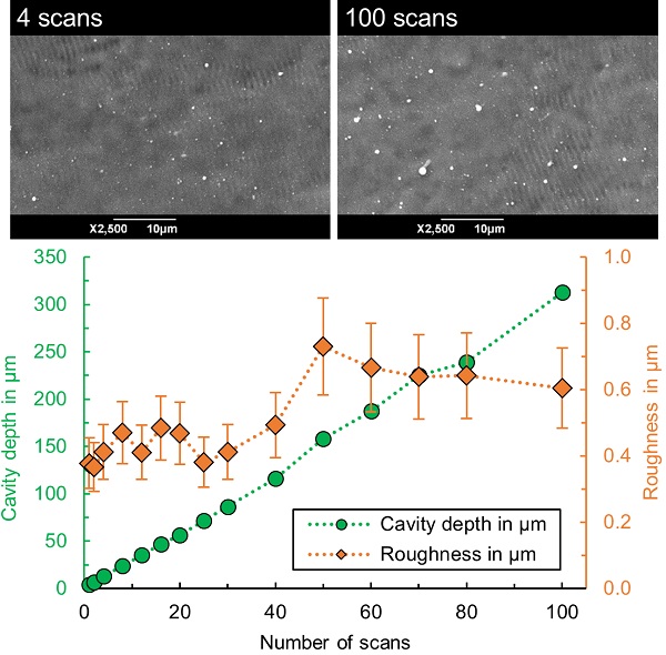
Figure 4: Cavity depth and roughness as a function of the number of scans and corresponding surface structure, via the micromachining of silicon with ultrashort laser pulses and 950W average laser power. (Image: Holder et al.)
The micromachining depth can easily be scaled due to the linear increase of the cavity depth with the increasing number of scans. In the present work, a low roughness Sa < 0.8µm and surface structure partially covered with fine ripples could be maintained up to the maximum micromachined cavity depth of 313µm. More detailed investigations and correlations on the influence of machining parameters on surface quality and removal rate in the micromachining of silicon have also been published5,6.
Demonstration
At an average laser power of 1.01kW, the machining strategy of low laser fluence and high-scanning speed demonstrated high-quality 3D micromachining using a wedge-shaped geometry with an area of 5 x 5mm² and continuous depth increase to over 300µm cavity depth (see left of figure 5).
The low average roughness of Sa = 0.6µm and low peak-to-valley roughness of 5.7µm over the entire wedge surface demonstrate a high-machining quality, thus a possible use in applications with high demands on surface quality. At the same time, a record-breaking throughput for micromachining was achieved with a very high material removal rate of 3.8mm³/s or 230mm³/min, corresponding to an increase of about a factor of 440 for comparable surface finishes. Due to the large machining field of 300 x 300mm², it was possible to produce large-area and high-quality surface structuring on silicon wafers (right of figure 5).
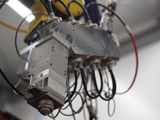
Figure 5: High-quality 3D micromachining and large-area surface structuring of silicon with ultrashort laser pulses and 1.01kW average laser power. (Image: Holder et al.)
Future work
These results show the great potential of high average power USP lasers in high-quality micromachining of semiconductors with high throughputs. Future research topics are the elaboration of strategies and development of technologies for the implementation of the high powers on the workpiece, for applications with smaller target geometries.
This project received funding from the European Union’s Horizon 2020 research and innovation programme under grant agreement No 687880.
