The silicon carbide (SiC) power device market is projected to achieve a compound annual growth rate of more than 30% to reach nearly $9bn in 2028[1]. Benefits of SiC power devices include boosting power efficiency and minimising energy loss in electric vehicles (EVs), hybrid EVs, power supplies, and solar and wind inverters. While much goes into the development of SiC power devices, the formation of ohmic contacts on the backside of these devices plays a key role in defining their electrical characteristics and mechanical strength.
Thermal annealing in the form of flash lamps has traditionally been used for backside ohmic contact formation (OCF). To form an ohmic contact with this method, a heat treatment of ~900-1000°C is applied to the wafer backside, causing the backside metal and the silicon from the SiC to form a metal silicide.
As the industry migrates to thinner SiC wafers (80μm thickness and below) to improve power device performance, thermal annealing is no longer feasible due to the high heat load generated on the frontside of these thinner wafers, which can damage the devices. Backside selective laser annealing with short-pulsed lasers is an attractive alternative due to their high precision and repeatability, and low thermal leakage, which prevent thermal damage to the wafer frontside.
Experimental setup of laser systems for OCF processing
3D-Micromac compared the process results of two different laser systems for OCF processing. Both are production systems equipped with a solid-state ns laser with a 355nm wavelength. The laser source of the first system has a Gaussian beam profile with TEM00 characteristics at the laser interaction zone. The pulse length of the single laser pulses is between 100-300ns. The process runs under oxygen-reduced atmosphere.
The second system was the new microPRO XS OCF built by 3D-Micromac. This system has an integrated 25 W ns laser with a pulse length between 50-100ns and a flat top profile with a diameter of 80μm. The benefit of a flat top profile versus a Gaussian beam is the homogenous energy distribution over the wafer. Furthermore, a larger laser spot size leads to increased throughput. A galvo scanner system guides the laser over the wafer’s surface. The process chamber is purged with nitrogen to reduce the oxygen level to <300 ppm.
Fully processed power electronic 4H-SiC wafers were used. The diameter of the wafers was 150mm. For wafer thinning, two different grinding processes (A and B) were used to check if there is an influence on forward resistance. A 75nm thick nickel layer was sputtered at the wafers’ backside. After the laser-based OCF, the wafers were cleaned, and the backside metallization stack was finished with a 4-5μm thick aluminium layer. After that, the forward resistance was measured for each device at the wafer level.
For this assessment, a run with six wafers with vertical resistor structures was performed. The wafers had a thickness of 80 and 175μm. For this evaluation, low forward resistance was the main quality criterion. With system 1, only one OCF parameter set was used. For the 3D-Micromac process, a parameter sweep was performed by varying pulse energy density and pulse overlap.
The results
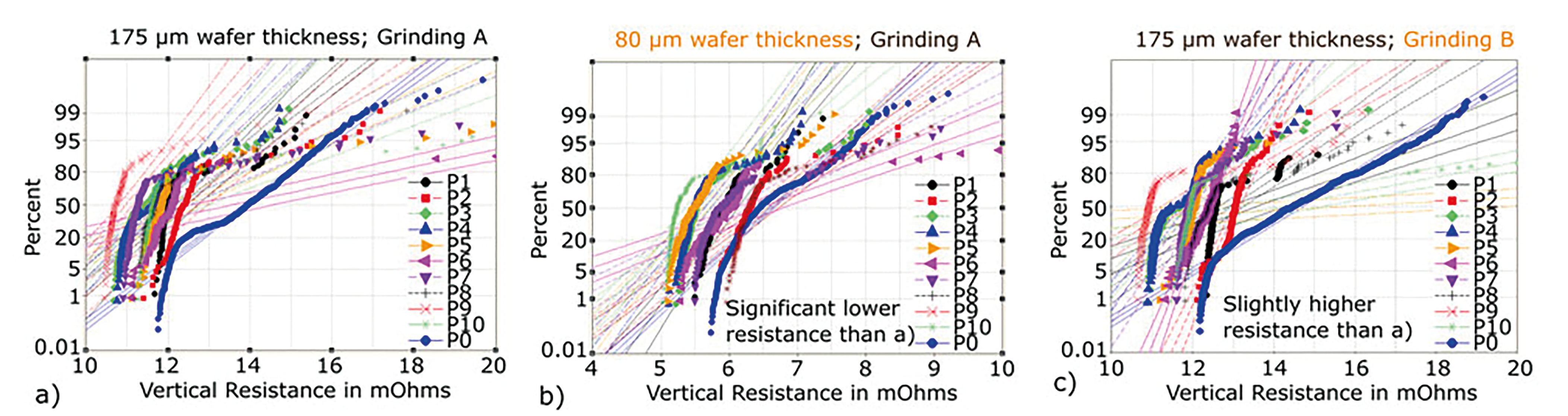
Distributions of forward resistance measurement on three wafer types. a) Grinding A with 175μm thickness, b) Grinding A with 80μm thickness, c) Grinding B with 175μm thickness. The aim is to reduce vertical resistance. The top hat processes (P1 to P10) of the microPRO XS OCF system show lower vertical resistance than the Gaussian beam process (P0) carried out by system 1. (Credit: 3D-Micromac)
The results of the top hat profile show a comparable or lower forward resistance compared to a Gaussian energy profile (Figure 1, above). In fact, all results generated by 3D-Micromac’s OCF process are similar to or better than the OCF process with system 1. Furthermore, an optimum forward resistance can be achieved by tuning the pulse to pulse overlap and the pulse energy density. A higher energy density or pulse overlap results in lower forward resistance. Nevertheless, an increase in throughput can be achieved by reducing the overlap.
About the microPRO XS OCF
The microPRO XS OCF selective laser annealing system was developed specifically for OCF processing. It provides a significantly higher throughput (up to 17 wafers per-hour) compared to competing laser annealing solutions. It achieves a surface roughness of only ~30 nm, which is critical for supporting subsequent process steps, and sheet resistance of ~0.5 Ohm/sq (depending on the conductivity of the base substrate). The process is highly uniform to within 1.1%. Both the process routine and process chamber have been designed to significantly reduce particle generation. The microPRO XS OCF is already being used in mass production of power devices and other applications.
Reference
[1] Power SiC 2023 Report, Yole Intelligence, August 2023, https://www.yolegroup.com/product/report/power-sic-2023/