Skip to main content
Social media links EO
LinkedIn
Twitter
Log in
Register
Applications
Life sciences
Environment
Quantum
Defence
Automotive
Aerospace
Medical engineering
Electronics
Optical communication
Technologies
Illumination & energy
Imaging
Industrial lasers
Lasers & optoelectronics
Sensors, test & measurement
Photonics 100
UK Photonics
Photonics Frontiers
Resources
Webcasts
White Papers
Supplier
Events
Products
Search
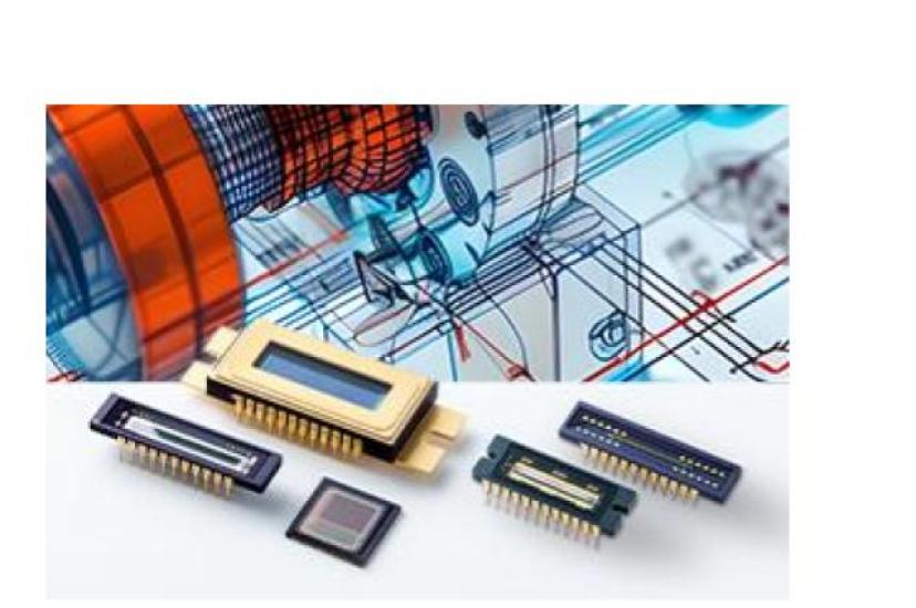
Advancing imaging technology with CCD sensors
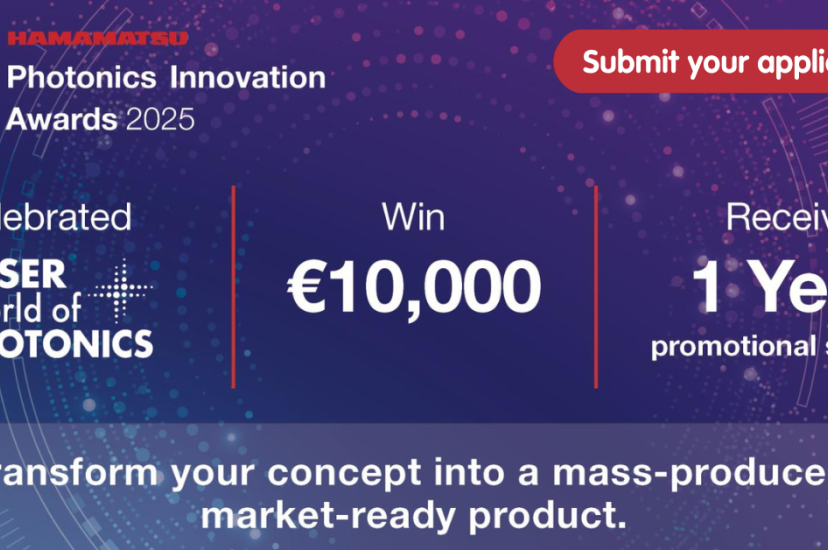
Searching for innovation: Announcing Hamamatsu's vision for photonics advancement
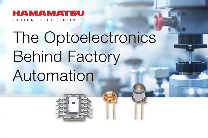
The optoelectronics behind factory automation
Hamamatsu Photonics purchases BAE Systems Imaging in strategic move
IonQ strengthens quantum computing ecosystem with photonic partnerships and strategic acquisition
Peter Seitz
Optoelectronic components market to be ~$64 billion by 2030
Diving into the essence of lidar technology
Hamamatsu and Vrije Universiteit partner on photonics industry innovation
Meeting optical communication demands with InGaAs photodiodes
Pagination
Previous page
‹‹
Page 4
Next page
››
Media Partners
")
")


")
")
")