Market theory postulates that, where there is a perceived customer requirement, then research and development will be directed to provide a solution to that particular problem; it is this, then, that is the driver for new technology. A modern example of this is the development, over the past 10 years, of miniature, low-cost CCD and CMOS image sensors, now a common accessory with most mobile phones. Today this is the major volume application for all image sensing devices.
Is this the whole story, however? Certainly not in the field of photonics, where most groundbreaking technologies were not developed with any perceived application or market in mind, but where visionaries wished to purely demonstrate what the science could do. There are numerous examples, but it is clear when Maiman and his colleagues developed the first lasers in the early 1960s, no-one envisaged mass data storage devices, bar code readers, and materials processing machines or optical telecommunications. Similarly, when fibre optic cables were invented in the early 1970s, no-one had the worldwide web in mind!
During the electronics manufacturing revolution that occurred in Japan during the 1960s and 1970s it is clear that the philosophy of following market needs dominated technology development and corporate expansion. However, Hamamatsu Photonics, a very small company back in those days, has always followed the second path. We try to develop the science that leads to new technology and new products, and from this the new applications and markets of the future will be created. This way of thinking has always made us stand out a little compared to most other companies in our industry and this allows us to consider R&D over a much longer term.
Of course, like all commercial organisations, we have to meet this year’s sales and profit figures but we have created a central research organisation with several different laboratories in Japan, which are completely devoid of these everyday commercial pressures. Nothing unusual in having a large R&D resource in the semiconductor industry, one may say, but what is different about the 150 or so scientists within our research laboratories is that none of them is directly developing new products or even new processes to make future devices! This, perhaps more mundane, development work is then left to the individual manufacturing groups within Hamamatsu to ensure they keep developing optical detectors, light sources, imaging products and so on.
Most effort within the research organisation is looking at how to apply both current and future photonic technologies and what kind of applications may result from this science. This is then more akin to a purer academic kind of research. Indeed as part of this effort, Hamamatsu sponsors a photonic science academy, a graduate university for individuals or small groups, dedicated to developing the science and technology that will be used for future photonics applications.
Different groups within our laboratories are looking at a multitude of future applications. PET (positron emission tomography) is a real-time nuclear imaging technique used for observing functional activity within the brain. It is a technique used for research into medical conditions, such as Alzheimer’s, as well as for fundamental mind-brain science. Applications of spatial light modulators are being investigated for opthalmic and medical diagnosis, as well as for parallel data processing, which could lead to future developments in optical computing. Laser diode technology is applied to use in agricultural production, materials processing and to aid in the development of future nuclear fusion technology. Photodynamic therapy (PDT) is a laser-based technique used to locate and destroy cancer in situ within a patient without the need for surgery.
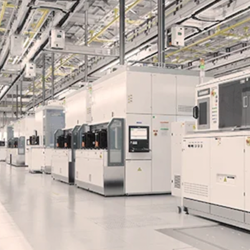
One example of where scientific product research has led to a real world application is in the field of today’s semi-conductor production. Back in the 1980s, Hamamatsu was researching various technologies related to UV laser light generation. The excimer laser was one such product that has found use in scientific and materials processing applications. Today new, unexpected applications have appeared in the semi-conductor field. With the precision control of an excimer laser beam, ‘stealth dicing’ technology today allows improvement in semiconductor yield, increased processing times and reduced die size, all resulting in lower cost ICs.
The President and one of the original founding members of Hamamatsu Photonics, Teruo Hiruma, has named this overall process of researching first and finding applications later ‘HSpiral’. The ‘H-Spiral’ process is defined as: new scientific endeavour leads to new technology, which creates new applications and new industries, and eventually to an improved standard of life for all.