Silicon photonic products are now on the market and the technology has reached a reasonably high level of maturity, but is still ‘several years out for wide-spread applications’, according to Dr Bert Offrein, manager photonics at IBM Research, Zurich.
The field has seen massive investment by the big semiconductor companies, largely because the electrical interconnect in microprocessors is nearing its limit in terms of bandwidth and power, explained Professor Graham Reed at the Optoelectronics Research Centre (ORC) at the University of Southampton in the UK. ‘Photonics was seen as one way forward, and now, silicon photonics is probably seen as the only way forward,’ he commented. Reed was Intel’s first consultant when the company entered the field around 10 years ago.
However, there still remain some critical issues to be solved, such as how to integrate a light source on a silicon chip in a way that makes full use of CMOS production technology, and how to package that chip and align it with an optical fibre. And while the big players like IBM and Intel have the resources for investing in the field, how can smaller companies take advantage of the opportunities that silicon photonics provides?
The products available commercially today are things like active optical cables, where two points are linked optically with an optical chip at the end. Luxtera is the company best known for these devices. However, there is a drive for higher levels of integration to make full use of CMOS production capabilities. ‘The big advantage of silicon photonics is that it builds on infrastructure that is available in CMOS manufacturing. This enables high-volume capability and will reduce cost and simplify integration into a system,’ explained Offrein.
One of the big hurdles is integrating the light source on a silicon chip. Roel Baets, a professor at Ghent University and head of exploratory research in silicon photonics at Imec, stated: ‘You can easily integrate modulators and germanium detectors in silicon. The integration of light sources in silicon photonics is a tougher job – it is considered by many as the Holy Grail.’
The issue is that silicon is not good at emitting light, so other materials have to be used. Most of the commercial products available today are based on hybrid laser chip integration, where a complete laser chip is attached onto the silicon wafer, either in a miniature package or by flip-chip technology.
The alternative is to bond III-V semiconductors such as indium phosphide (InP) onto the silicon platform. ‘The problem with bonding technology is that by definition it cannot be a full wafer technology,’ explained Baets. Standard silicon wafers are 200mm and 300mm, whereas such wafer sizes don’t exist in the III-V world – wafer sizes in InP are typically 75mm to 100mm. ‘There is a wafer size mismatch, which means several smaller or larger III-V dies have to be bonded onto the silicon platform,’ he continued. ‘That makes it a technology which is much less directly compatible with what is available in a CMOS fab.’
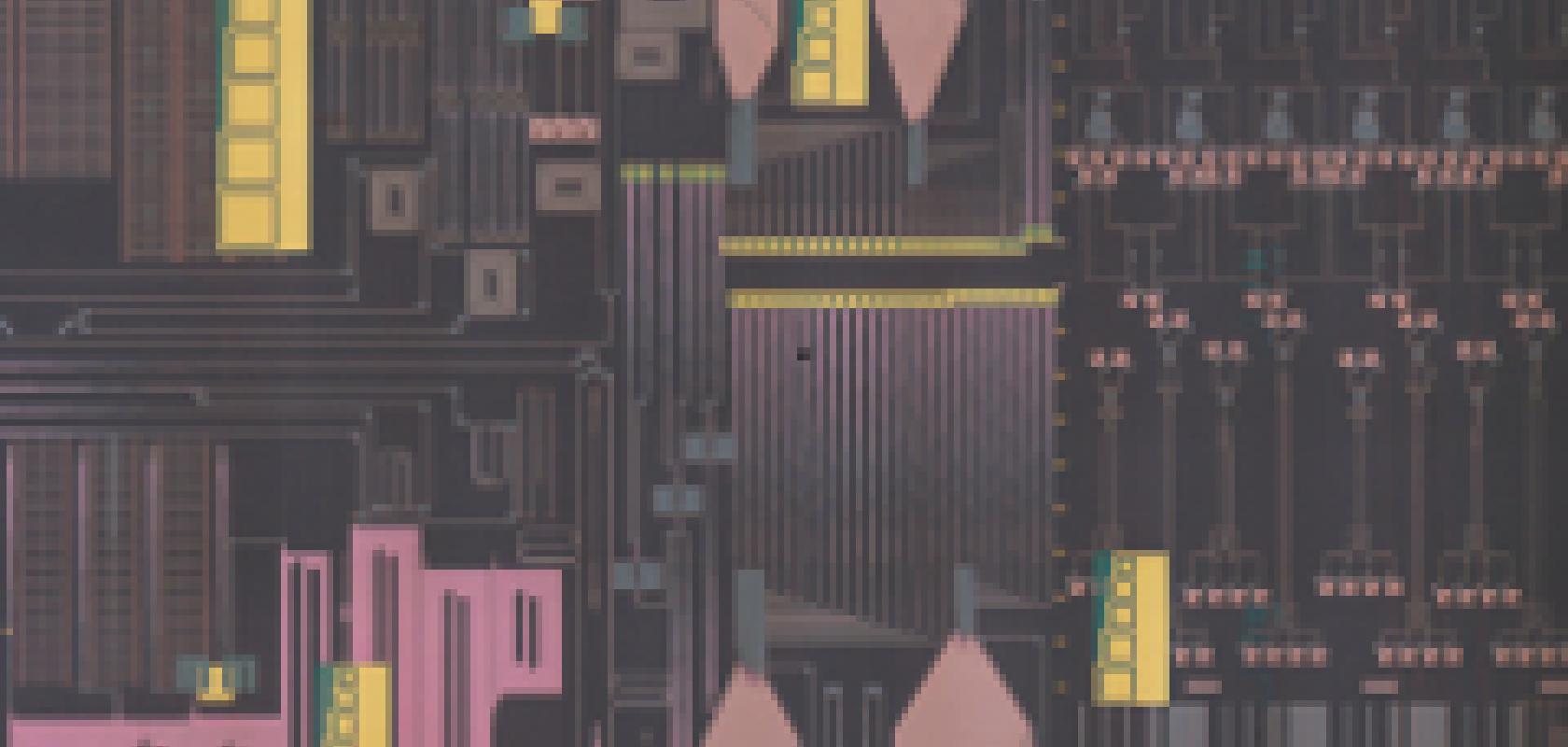
Imec’s silicon photonics platform offers passive functions, but also active photonic devices including high-speed modulators, detectors, and the heterogeneous integration of III-V lasers on silicon.
The III-V wafer is bonded with its epitaxial layer structure upside-down onto the processed silicon wafer. Then the InP substrate is removed. What remains is thin, III-V epitaxial layers bonded onto the silicon circuitry, which, since it is a planar wafer at that point, can be processed in a full wafer fab. The processing of the laser is carried out at the wafer scale, but the actual bonding step itself is a multiple die-to-wafer attachment process.
‘Several groups in the world have mastered this technology quite well and have integrated lasers on silicon with respectable performance,’ commented Baets. ‘However, the technology so far hasn’t been brought to industrial maturity. Intel has gone a long way in doing that. But still there are hardly any CMOS fabs in the world where you could have these integrated lasers being processed on the silicon at the moment.’
There is also a third option, which is still much more at a research stage and far from maturity, but if it materialises then it might prove to be the winner in the long run, according to Baets. This is to grow III-V semiconductor material directly onto silicon – not bonded, but epitaxially grown. This has been notably difficult, because there’s a large crystal lattice size mismatch between silicon and, for example, InP, along with various other issues. Therefore, in the past, growing InP directly on silicon resulted in very poor-quality material that was full of defects.
But in recent years there have been several groups reporting successes in reaching good quality crystalline material, according to Baets. ‘There is an increasing interest in direct growth of III-V on silicon – and, if that is possible, then you have a potential route towards full wafer technology in a CMOS fab including the laser. It’s something not yet mature, but there are optimistic signs in recent years that it might be realistic.’
IBM has an interest in silicon photonics for data centre applications and high-performance computing. ‘For IBM, big data is a very important aspect. Here, high-bandwidth, efficient communication within and between data centres is important,’ commented Offrein.
IBM’s silicon photonics platform combines both electrical and optical functionality, which, according to Offrein, is different to what many others are doing in this area. ‘We want to bring the critical electrical circuitry very close to the optical devices they are driving,’ said Offrein – so the driver circuitry is physically close to the electro-optical modulators and the amplifiers are close to the germanium detectors. ‘Such a short distance means you have optimum performance, and we can design the components in such a way to have an ideal match.
‘What we’re [IBM] exploring in research is: what is a reasonable path in order to move towards tighter integration of the laser on silicon? Today, it’s a separate laser, but we see large potential in bringing the laser onto the chip,’ Offrein commented.
It used to be that CMOS fabs would regard any form of III-V material as an impurity, but as they started moving towards ever smaller nodes, like 14nm and 8nm, III-V began to be needed to make higher-performance transistors. Dr Jens Hofrichter, a postdoctoral researcher at IBM Research, Zurich, noted that, by building on this, the CMOS community can start thinking about integrating lasers onto silicon photonics using the same technologies and methods.
Letting the heat out
The light source challenge is complicated further by the temperatures the lasers would have to operate at as part of a data centre application, for instance. Dr Dennis Deppe, a professor at CREOL, the College of Optics and Photonics at the University of Central Florida gave a presentation at the beginning of May at IEEE’s Optical Interconnects Conference in California, USA, titled: ‘Letting the heat out: silicon photonics integration with VCSELs’.
Dr Deppe is working on integrating vertical-cavity surface-emitting lasers (VCSELs) on silicon chips. ‘In some ways VCSELs are viewed as competition for silicon photonics,’ Deppe told Electro Optics. ‘I view them as a laser device for silicon photonics, because I see advantages in integrating those lasers with silicon electronic circuitry.’ According to Deppe, most of the big applications for silicon photonics, such as data centres and high-performance computing require high-temperature operation. ‘The laser has been a big barrier, because a lot of the lasers that are being implemented and the ways that they’re being implemented don’t allow the lasers to work at high temperatures,’ he said.
There has been previous work integrating VCSELs on silicon CMOS, mainly in a free space manner, but also using waveguides. ‘It’s really when you start implementing electronics on the chips to make them more powerful in terms of their capabilities, that’s when you run into the problems of the electronics generating too much heat,’ Deppe continued. ‘In addition, the applications that these silicon photonics chips are being used for also generate a lot of heat, where the chips are packed densely with a lot of other packages. The thermal barriers are quite large in terms of what kinds of laser can actually work for this.’
Deppe believes that VCSELs are the best option to overcome the thermal barriers for efficient laser operation. VCSELs have good temperature performance and, according to Deppe, CREOL has the best temperature performance of any VCSELs. VCSELs also have extremely fast modulation.
Reaching a mass market
Professor Reed at the University of Southampton is leading a research project that is looking at some of the challenges in bringing silicon photonics to a mass market. The group was awarded a £6 million grant by the Engineering and Physical Sciences Research Council (EPSRC) in the UK, with the project beginning at the start of 2014.
The project will investigate five areas, which were chosen, according to Reed, because they were areas that are crucial for commercialisation, yet have been less intensively investigated because most of the work has been focused on improving the performance of the technology. Consequently these are also areas where the group felt it could make a big impact in the field.
The first area is looking at low-cost methods of integrating lasers on a chip with other photonic devices, although Reed emphasised that this won’t encompass making a silicon laser. Secondly, it will investigate integrating modulators and increasing the aggregate data rate of optical transmission chips. The group is working in collaboration with Sharp to produce a chip for future generations of HD TVs, and with Oclaro for very high aggregate data rate photonic circuits.
The third area is developing multiple photonic layers within a silicon chip – two or more layers, Reed specified – to improve the functionality. ‘You could produce layers that have different optical characteristics and also, with two layers, you could double the functionality, and perhaps you might do better than that because these layers could interact with each other,’ he explained.
The fourth area is developing wafer-scale testing for a silicon photonics chip, with which the group has already had success. This is more difficult to do optically than electronically – probing electronically is, in principle, relatively simple, because there just needs to be an electrical contact. Optically, it’s more difficult because the light has to be coupled in and out, so any probing point created in the middle of a circuit to test just one component would also be a loss point for the light after testing is complete. In this area, the group are collaborating with industry partner Wentworth Technologies.
The group has demonstrated a potential solution to this problem, by forming an erasable grating to couple into the circuit. ‘We’ve found a way of changing the refractive index in a periodic way that we can subsequently erase,’ Reed said. That means a probing point could be introduced to test the circuit, and then erased afterwards by local laser annealing.
The final area will be to investigate how to align silicon photonic waveguides, which are sub-micrometre in size, with optical fibres that typically have a core diameter in the order of 10µm, and to do this in a passive way. To have a mass production technology, there has to be passive alignment, noted Reed. This is something IBM is also working on, taking the approach of integrating grating structures in the silicon in order to couple light from the waveguide to the fibre.
In addition to this grating coupling approach, IBM is also working on a method to scale up the whole packaging design to integrate many input and output optical signals on the silicon chip. The company also wants to do that, in the longer term, over a broad wavelength range. In a paper published in 2013, IBM demonstrated one potential concept to do this, which is based upon integrating a short stretch of polymeric waveguide technology, around 1cm in length, in between the fibre and the silicon chip. The polymeric waveguide converts the very small modal field size – the very tight confinement of light in the silicon waveguide – to something that can be easily coupled to a fibre. In addition, such a concept can be scaled up to a larger number of inputs and outputs.
Money talks
International companies like Intel and IBM are spending vast sums on investigating and developing silicon photonics, which smaller companies and research projects would find hard to compete with. Baets at Imec commented that the market for transceivers for short reach datacom applications is typically addressed by big players. ‘You can’t enter the market for high-speed transceivers as an SME. You must be an Intel or a Samsung to enter this market,’ he said. ‘It would be a shame if this wonderful technology that is silicon photonics would only be deployed for these very large volume applications.’
Baets explained that getting silicon photonics wafers processed in a CMOS fab is expensive. The chips themselves are cheap because so many are made per wafer and processed in large batches, but, in his opinion, there needs to be a supply chain where moderately sized applications can make use of this technology.
There are already mechanisms that make this possible, but mostly they occur in a research or prototyping context, he said. Here, groups run the processing in multi-project wafer (MPW) mode, where the designs of a number of users are aggregated onto a mask set. The chips are then processed collectively and the wafers distributed to the various users. ‘In that mode, you can have a substantial cost sharing of the whole process,’ Baets remarked. ‘This has been common in microelectronics for the past 30 years. So, it’s a model that’s well-known to the CMOS community and it can also be applied to silicon photonics.
‘To date though, the MPW model is limited to research and prototyping, but is not yet fully industrial for silicon photonics,’ he added. ‘That’s [MPW processing] certainly one of the things that will have a huge added value for a variety of markets, especially in sensing and life science applications.’
Hofrichter at IBM agrees: ‘One of the reasons for the success of electronics is that electronic building blocks, essentially transistors, are so standardised, which is currently not the case for optical components.’ He said that in order to enable a broader market, standardisation is needed, not only for the components on chip, but also for packaging. ‘It’s crucial that the packaging is standardised so the cost goes down,’ he added. ‘In the future, more multi-project wafers would dramatically drive the cost down. Currently, this is not our primary focus at IBM, but it could enable a broader market to be accessed.’
Professor Reed commented that the presence of huge multinational companies in the field has increased enormously in the last decade, and is a very good thing. ‘The difference between silicon photonics before these massive companies were involved and now is that it’s moving much more quickly. Not just because the big players are putting big money in, but because it’s focusing people’s minds on applications. You can see that if you produce something significant in this area, then there’s a good chance that it might get exploited, which focuses your mind on what the real challenges are.’
Reed added: ‘Overall, the whole field is massively buoyant. It does mean that there are a lot more players in the field, but it also means that there is a lot more innovation and a lot more interest, and if you’ve got some good stuff to offer, the chances of making an impact are enhanced.’’
 Greg Blackman is the editor for Electro Optics, Imaging & Machine Vision Europe and Laser Systems Europe.
You can contact him at greg.blackman@europascience.com or on +44 (0) 1223 275 472.
Find us on Twitter at @ElectroOptics, @IMVEurope, and @LaserSystemsMag.
