Wafers with inset of soft mark detail.
The traditional production method for printed circuit boards (PCBs) requires making a series of photo-tools; masks that contain the pattern of circuit elements and components for each layer of the board. The pattern of components is transferred onto the PCB by first coating the board in a layer of a chemical that reacts with UV light, called a photo-resist. Light is projected through the photo-tool onto the photo-resist-coated panel. The chemical reaction with the light etches the component pattern into the board.
However, this approach is not so useful for creating extremely fine detail, as required on many modern circuits and semiconducting chips. Problems such as registration errors between the PCB layers may occur because the materials used for the mask and panel (such as FR4 and Teflon) expand and contract as ambient temperature and humidity changes. Photo-tools can also be damaged or contaminated easily, leading to errors in the final pattern, if not handled and stored correctly.
Laser Direct Imaging (LDI) is an alternative method of creating PCBs that overcomes these limitations. LDI systems, such as those offered by Israeli firm Orbotech, use lasers to etch a circuit pattern directly on to a photo-resist-coated panel. The instrument's controlling computer is first loaded with the desired circuit pattern, and then used to control a focused laser beam that is scanned sequentially across the panel. After etching is completed on one side of a panel, the panel is flipped and the second side is processed. LDI devices of this type currently available can scan panels up to 60cm wide in a single pass, eliminating the need for stepping or stitching.
Because LDI does not employ a physical photo-mask, the dimensions of the pattern produced with the laser are not affected by ambient environmental conditions. The flexibility of the LDI method also allows the size, orientation and shape of the written pattern to be varied as needed to maintain optimum registration. Any required transformations in the imaged pattern are determined by measuring the positions of features on the panel. LDI can render details down to 24µm in size on the production line, doubling the quality achievable over traditional production methods. LDI avoids any quality problems associated with film-related defects and handling and storage of photo-tools.
Orbotech's LDI systems are based on Coherent's Paladin series of lasers, which are mode-locked, diode-pumped solid-state lasers with an output up to 8W at 355nm. The Paladin lasers operate at a wavelength compatible with photo-resists commonly used for contact printing, which were originally activated with mercury arc lamps. The output power of the Paladin is also high enough to allow it to be used with lower sensitivity, less expensive dry films.
Many companies supply optical components to control the laser beam used for direct laser etching. For example, LIMO supplies beam shapers and homogenisers that allow even finer detail to be created during semiconductor manufacture. Laser-Laboratorium Göttingen manufactures a variety of phase masks, ranging from simple structures such as 1D- or 2D-gratings and beam shaping optics, to complicated structures. They can be used with many different wavelengths, from infrared to ultraviolet.
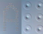
A character of a soft mark is composed of a series of dots, each one created by a single laser pulse.
Semiconductor wafer manufacturers often place small marks on their un-patterned wafers, in order to allow tracking and identification of each individual unit through subsequent process steps. Laser marking can also be used to etch serial numbers, or other identifying marks, such as batch numbers, on to the finished components. The marks are usually either human readable alphanumeric characters, or bar codes, readable by machines. The marks themselves consist of a series of small dots, each created by a single laser pulse, placed close together, but not overlapping. While a deeper mark is more legible and less likely to become obscured after a number of process steps, it is also more difficult to clean out debris that could become temporarily trapped in the marks. Instead, manufacturers use shallow markings called soft marks. This is particularly important when being used to mark electronic components, as such debris could cause components to malfunction by forming undesired connections between the very small circuit pathways. Deep marks could also change the bulk electrical properties of the silicon surrounding the mark.
German firm Innolas builds soft marking tools for semiconductor manufacturers. The Innolas system uses galvanometer mirrors to scan the focused output from a pulsed laser on to the wafer surface for marking. Innolas use a Coherent PRIMSA series, q-switched, diode-pumped Nd:YAG laser for the process, which is computer-controlled to allow marks to be produced on the fly.
Rofin produces laser systems used for engraving, marking, and micro machining electronic components. For example, Q-switched YAG lasers from Rofin are used for laser dicing of QFN (Quad Flat No-lead) or MLFP (Micro Lead Frame Plastic) packages for electronic components. This means the device is manufactured without conventional leads to connect it to a PCB. The devices can be mounted directly to the surface of the PCB, allowing a higher density of components on a board. This method also reduces lead inductance is (permitting higher operating frequencies) and enhances component cooling. This form of component packaging is popular in mobile phones and PDAs.
A microprocessor starts its life as a segment of a large wafer of semiconductor material. However, before the chips can be etched, the wafer must be checked to ensure that it meets the requirements for microchip manufacture; the producer must be sure that the surface is not unduly rough, and that the structure of the material does not contain any defects.
Taylor Hobson uses a method of non-contact metrology called coherence correlation interferometry (CCI) to examine semiconductor wafers. The TalySurf CCI 3000 measures the phase relationships of light reflected from the surface being measured, and generates a three-dimensional image of the surface. The TalySurf has a vertical resolution of 0.1Å and lateral resolution of 0.36µm.
Strained silicon is a form of the popular semiconducting material in which the atoms are slightly further apart than those in normal, unstrained silicon.
This allows electrons to flow through the material with less resistance. Intel's latest processors use strained silicon to increases transistor drive current which, in turn, improves switching speed by making current flow more smoothly.
Verifying the quality of materials such as strained silicon relies upon being able to check the atomic structure. Imaging at this scale requires special techniques. For example, Nanonics Imaging produces Raman spectroscopy devices that are able to characterise atomic nanoscale structures, whereas the British firm Bede produces systems for x-ray metrology.
It is no exaggeration to suggest that advances in semiconductor technology in general, and microchips in particular are driven by advances in manufacturing quality and techniques. As laser processes and photonic techniques become more widely used in industry, so finer detail can be etched into raw semiconductor materials.
