The helium-neon laser was invented in 1961 and still forms the basis for many optical metrology techniques. However, semiconductor laser diodes now offer higher powers and a broader range of wavelengths compared to the fixed 632.8nm of the HeNe laser, both of which could see the diode laser start to replace older HeNe technology.
Dr Christian Nölleke of laser company Toptica Photonics will give a presentation on the metrology applications for diode lasers as part of the high coherence metrology panel on 24 June at Laser World of Photonics in Munich, Germany. Dr Patrick Leisching, vice president of R&D at Toptica, spoke to Electro Optics: ‘The HeNe laser is a gold standard and also an official secondary frequency standard for metrology systems, emitting at 632.8nm. There are options available now, however, of diode lasers that emit in the UV wavelengths, which give more accurate measurements.’
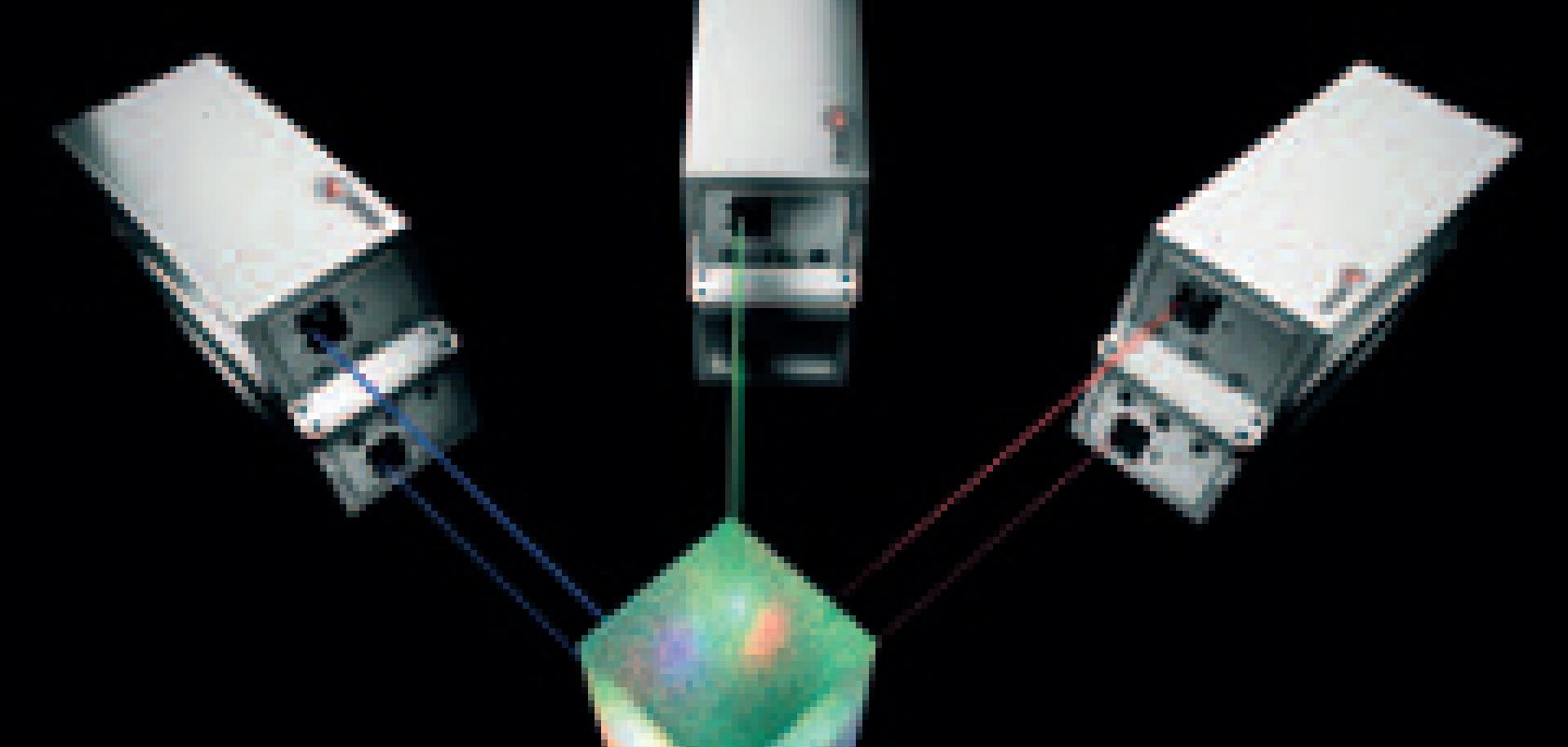
Toptica’s TopMode laser, for instance, emits at 632.8nm, 515nm or 405nm. It can also produce 100mW of power – ‘not only can you go to shorter wavelengths, but also to higher powers with semiconductor lasers,’ Leisching said. Furthermore, semiconductor lasers can be modulated and tuned, which are additional advantages for metrology.
The downside to diode lasers is that they need to be stabilised for metrology applications, which requires the addition of a gas cell. HeNe as a lasing medium, on the other hand, is inherently stable. So, semiconductor diodes are good for relative measurements and have many advantages like the broadband emission, but they need external stabilisation of the wavelength.
‘In the mid-90s, there were millions of HeNe lasers sold per year,’ Leisching remarked. ‘This number fell with the introduction of the semiconductor laser, which replaced HeNe lasers mostly in the low-end market segments. Today the market for HeNe is around 25,000 per year, mostly in high-end applications like metrology.
‘The driving force for changing to semiconductor lasers from HeNe is the fear from the test and measurement industry that the HeNe technology is too old and will fade away,’ he continued. ‘In addition, the driving force is definitely the semiconductor industry – they want to keep the 632.8nm wavelength, but they need more power.’
The higher laser powers address the need in semiconductor fabrication to make measurements at the nanometre scale, while at the same time covering larger wafers that can reach 300-450mm in diameter. Boosting the power from a 1mW HeNe laser to a 100mW diode at 632.8nm would give big benefits in metrology for semiconductor production. ‘Just having higher powers reduces the measurement time and you can measure more accurately,’ Leisching said. The second option is go to UV wavelengths – the shorter the wavelength, the higher the accuracy.
Non-contact metrology techniques are applied at various processing steps in fabricating a silicon chip, not all of which use lasers. One potential application within the semiconductor industry is measuring the active thinning of silicon wafers, a task that Precitec Optronik’s CHRocodile sensors would be ideal for, noted Ian Johnstone, sales and marketing director at Armstrong Optical. Armstrong Optical is a distributor of the Precitec systems.
One of the process steps is to deposit a layer of photoresist onto a silicon wafer and then etch away the exposed silicon in an acid wash. ‘Currently manufacturers simply time the treatment to estimate how much of the silicon is etched away. You want to be able to look at the wafer in real time and watch its thickness vary a nanometre at a time. That’s what the Precitec sensors can do in the near-infrared, with the sensors actually submerged in the acid wash bath,’ Johnstone said.
The CHRocodile sensing technology is based on chromatic confocal (to measure distance and thickness) or interferometric principles (to measure thickness), using a broadband white light source. A fibre feeds the illumination to an optical head designed to introduce either chromatic aberration down the optical axis (chromatic confocal) or simply focus (interferometric). The sensor produces a spectral continuum between the blue and red focal points, which then defines the working range, varying from as small as 100µm up to 25mm. Any surface in that chromatic field will reflect back into the sensor the wavelength, which is a function of its position within the field. The returned, almost monochromatic, light is measured with a spectrometer to give a peak corresponding to the distance from the end of the sensor to the object surface. The 100µm optical probe has a resolution of 3nm, while the 25mm system has a 1µm resolution.
The device can not only measure distance, but also the thickness of a material. ‘If a transparent object is placed in the working range you’re going to get a return of one wavelength from the front surface and a return of a different wavelength from the back surface. If you know the refractive index you can work out the thickness of the material,’ explained Johnstone.
The 25mm working range optical probe, which has a working distance of around 78mm, is currently being used in the glass container manufacturing industry to measure wall thickness in bottles. A glass bottle producer in the UK uses the Precitec sensors to measure the bottle heel thickness, where the container wall becomes the base, and the shoulder, where it can contact other bottles in the packaging. The two measurements are performed around the complete circumference, in real time, as the bottles come down the production line at 350 bottles per minute.
‘There are other methods of measuring bottle thickness in real time, including those based on laser triangulation. However, they tend to fall down when you’ve got deep indentations, so heavily patterned glass bottles,’ noted Johnstone. In addition, the Precitec sensors can measure coloured glass or even opaque bottles, and are unpowered meaning they can be used safely in hazardous environments.
Precitec has recently introduced the CHRocodile Chromatic Line Scanning (CLS) system, which deploys 192 measurement points arranged in a line varying between 1mm and 5mm in length. The CLS version is designed for high speed area scans, such as for measuring micromechanical components or features in electronic circuitry. The sensor provides data acquisition at up to 384,000 points per second with nanometre-scale resolution.
Frequency combs
As part of the high coherence metrology application panel at Laser World of Photonics, Dr Ronald Holzwarth at Menlo Systems will give a presentation on femtosecond lasers and optical frequency combs, technology necessary for extremely precise measurements. Frequency combs of the kind made by Menlo Systems or Laser Quantum can be used to calibrate lasers for interferometric metrology to nanometre accuracy operating over distances of kilometres.
‘Frequency combs can conduct length measurements on any scale, from the nanoscale to millions of kilometres – there are proposals out there for measurements between satellites in space,’ explained Dr Michel Mei, CEO of Menlo Systems. ‘Some of the applications still have to be proven, but in theory frequency combs can work on any scale.’ In April, one of Menlo Systems’ optical frequency combs was sent into space as part of the Texus 51 mission for measuring different clocks in microgravity.
The output of an optical frequency comb is made of discrete laser lines whose frequencies can be controlled and measured with extreme precision. Such optical frequency combs can be used as a ruler in frequency space with hundreds of thousands of markers along the frequency axis. Any laser can be stabilised to it and the resulting length measurements have a high accuracy because the comb itself is extremely accurate.
The comb is based on a femtosecond laser oscillating at high optical frequencies – green light is around 560THz. The repetition rate gives the distance between the modes in frequency space, and the offset frequency gives the absolute position of all modes against a zero, for example. ‘It requires a stable laser, but it also requires active feedback to these two degrees of freedom,’ explained Mei. ‘The more accurate and more stable the laser is in the beginning, the easier the task of active feedback. The heart of the whole system is an intrinsically low noise, very stable laser – Menlo has developed its own femtosecond fibre laser for its frequency combs.’
Industrial measurements
The optical metrology techniques used in industrial processes are varied and wide ranging. Devices such as Sensofar Metrology’s 3D optical sensor, S Mart, which combines confocal, interferometry and focus variation techniques to give measurement resolution down to 0.1nm, or Attocube’s displacement sensor IDS3010, which offers position resolution of one picometre via interferometry, are both designed for industrial metrology applications. The Sios laser interferometers, supplied by Armstrong Optical, are also industrial equipment, employing a HeNe laser and a telescope arrangement to measure continuously over 80 metres with a resolution of 1nm.
Newport company, Optimet, bases its sensor technology on conoscopic holography. The sensor is collinear, i.e. light travels to and from the object on the same axis, which means it can inspect the inside of boreholes including the sidewalls without occlusions. This can’t be done with triangulation, where a laser line is projected at an angle.
‘The technique is also ideal for building up a 3D profile of part geometries that would otherwise be difficult to measure,’ said Shmulik Barzilay, international sales manager at Optimet. ‘The sensor can cover a round bowl with ±85° of coverage; this is compared to triangulation, which would have only around half the coverage, approximately ±40°.’
Optimet has customers in France that make engines for aircraft and automobiles that use the sensor to measure the internal dimensions of holes in the engine. The other big area for the sensors is in dental scanners for creating 3D scan profiles of gypsum models and teeth impressions in order to produce CAD-CAM prosthetic parts.
The sensor contains an anisotropic crystal which splits laser light returning from a surface into two beams with orthogonal polarisation modes. As the light leaves the crystal an interference pattern is generated, the fringes from which can be translated into a distance measurement – the distance between the sensor and the object can be calculated from the frequency of the fringes. In this manner, the sensor generates a point cloud and a 3D profile of the object’s surface.
Optimet has point sensors, which are very accurate but only cover a small area. The company is also launching a line sensor with a rotating mirror, which is accurate down to a few microns. ‘This is a level of accuracy which usually only can be achieved with point sensors,’ said Barzilay. ‘In addition, the line sensor can scan larger areas much faster – it has a scanning speed of 20kHz.’ The line sensor would be ideal for scanning larger parts, such as making flush and gap measurements in automotive applications.
Optimet’s sensors can also be calibrated with different lenses to measure over different distances – a 16-250mm lens can be fitted to the same sensor head to get a diverse working distance. ‘If you want very high accuracy – 1µm, for instance – you have to be very close to the object. At 20mm you might get 1µm accuracy,’ explained Barzilay. ‘If you need a large standoff distance – if the object is large, for example – the accuracy will decrease.’
Other presentations in the high coherence metrology application panel at Laser World of Photonics include distributed acoustic sensing in the oil and gas industry using fibre optic technology, as well as fibre lasers for interferometric sensing.
In terms of the increasing use of diode lasers in metrology applications, Leisching of Toptica noted one future potential use of semiconductor diodes for making measurements is within quantum communication, which requires a very accurate and tuneable light source. Toptica is working in collaboration with some of the UK universities taking part in the UK Quantum Technologies Programme, where there are projects designing detection systems at 780nm for diverse applications such as detecting submarines or the metal resources underground for mining. ‘You could build very accurate advanced detection mechanisms with gas cell stabilised laser diodes,’ he said. There are also medical applications at 850nm, such as sensitive devices for cardiology.
 Greg Blackman is the editor for Electro Optics, Imaging & Machine Vision Europe, and Laser Systems Europe.
You can contact him at greg.blackman@europascience.com or on +44 (0) 1223 275 472.
Find us on Twitter at @ElectroOptics, @IMVEurope, and @LaserSystemsMag.
