Experimental work on a number of novel light sensing materials is opening up their potential use as new materials for optical sensors. Recent research has found that materials not often associated with the world of optical sensors could actually unlock the potential for fast, high-performance and easy-to-manufacture devices by exploiting previously dismissed characteristics.
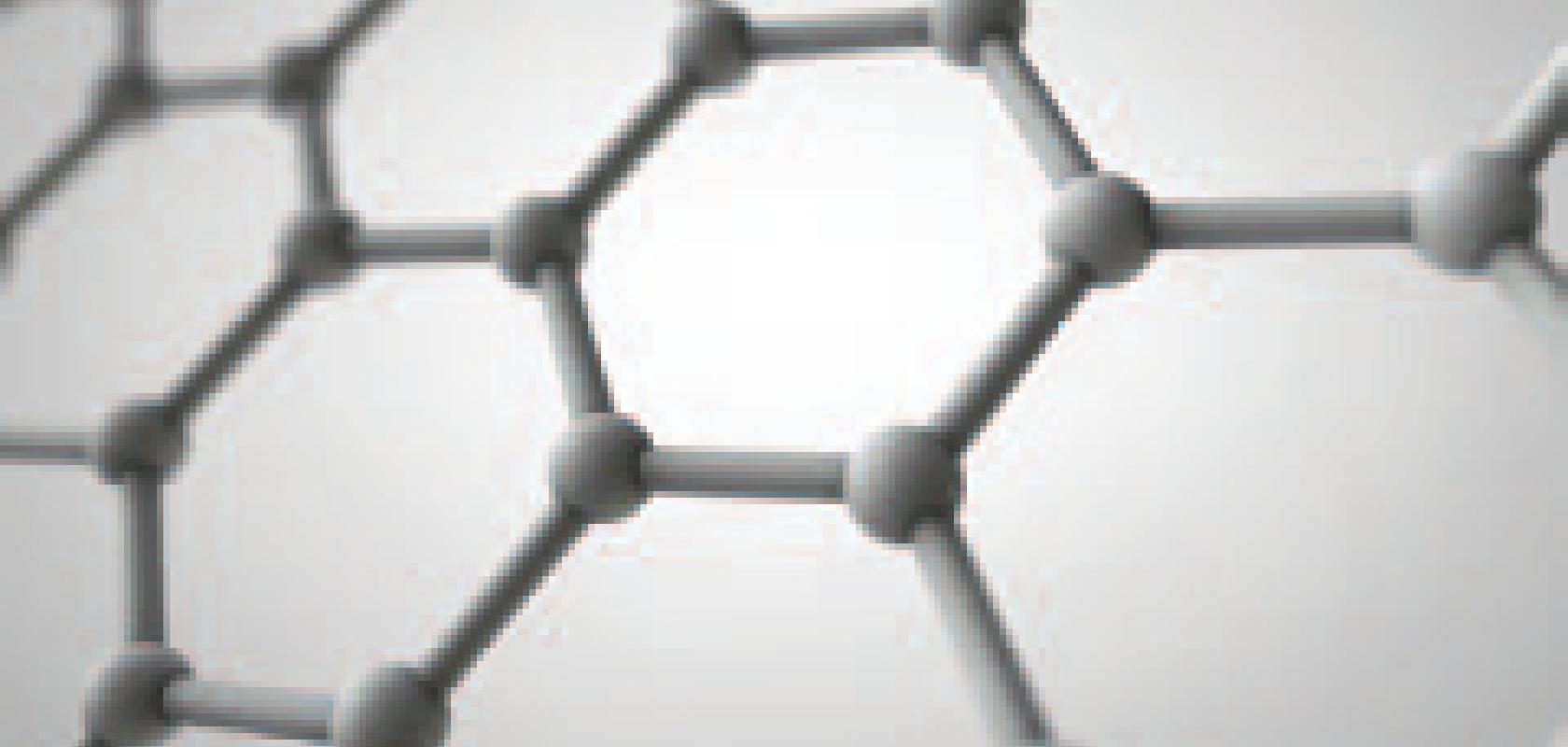
One such candidate is graphene, which has previously been considered a promising material within the world of optical sensors due to its ability to absorb light over an incredibly broad range of wavelengths. But research is now targeting a different effect, which brings with it a range of new applications.
Graphene can be used in devices that are based on the photo-thermoelectric effect. Here, absorbed light produces excited electrons, which very rapidly exchange energy with the other electrons in the conduction band. This leads to the electron system heating up, with the elevated electron temperature driving electron flow through a phenomenon known as the Seebeck effect. This effect is highly efficient in graphene due to the material’s large Seebeck coefficient.
A recent study based at the Institute for Photonic Sciences (ICFO) in Barcelona found that the processes of absorption, electron heating and photovoltage creation in graphene are highly efficient and extremely fast, happening at timescales of around 50 femtoseconds. This work could therefore pave the way for an ultrafast photodetector made from the material.
In addition, the efficiency of electron heating means the signal is relatively large and that the responsiveness is flat over a wide range of wavelengths. This is in contrast to conventional detectors that have a higher responsiveness at longer wavelengths.
Dr Klaas-Jan Tielrooij, research fellow at ICFO, spoke to Electro Optics: ‘This is a very different approach than most conventional photodetectors that use the photovoltaic effect, where electrons and holes are separated in a built-in electric field, which creates a photocurrent.’
The most obvious application would be the development of extremely broadband femtosecond autocorrelators – detectors that measure the duration of light pulses.
Tielrooij said: ‘An interesting application could potentially also be telecommunications, where high-speed photodetectors are used to convert optical signals into electrical ones.’
However, for such applications, the speed is not determined by how fast the signal is generated – on the order of less than 50fs as observed by Dr Tielrooij, Professor Frank Koppens, Professor Niek van Hulst and the rest of the team – but also by how fast graphene recovers from this effect, which is typically around picosecond timescales.
Tielrooij added: ‘More research will be needed to utilise the femtosecond signal creation for such applications.’
Caught in a trap
Recent research has exploited charge trapping defects, which are usually problematic within optical sensors, to improve the sensitivity and responsiveness of a novel light-detecting material.
The study, from the University of Nebraska-Lincoln and the National Institute of Standards and Technology (NIST), focuses on films of Organometal Trihalide Perovskites (OTPs) and suggests that defects present in these materials could be harnessed to develop high-performance optical sensors at a low cost, thanks to the ability to process such films easily.
Until recently, other investigated materials have been hampered by poor carrier mobility, which is the inability to conduct light-generated electrical charges efficiently. However, the research reveals that the carrier mobility of OTPs is comparable to that of crystalline silicon.
When a light-sensitive material absorbs a photon it transfers energy to a negatively charged electron. This then goes into an excited state and leaves behind an empty hole which is positively charged. These oppositely charged carriers must travel in opposite directions to different electrodes for high carrier mobility, but defects that trap either electrons or holes reduce the carrier mobility and reduce an optical sensor’s performance.
Conversely though, such surface defects and traps that exist close to the electrodes in OTPs can boost an optical sensor’s performance.
Optical sensors detect light by measuring the changes that occur in a material when a photon hits it. One way to increase the sensitivity is to apply a voltage and these defects, or traps, located near the electrodes lower the energy barrier for injecting electrons.
Dr Jinsong Huang, associate professor at the University of Nebraska-Lincoln, told Electro Optics: ‘Usually we want to get rid of these defects but we found that when they are present at the interface, a large photoconductive gain is produced that amplifies the signal and this leads to a greatly enhanced detector performance.’
This multiplying effect is only observed if the traps are located in proximity to the electrodes, and not throughout the material. This large amplification requires a very low voltage, on the order of 1V in OTPs, so these highly sensitive optical detectors could be integrated into low power circuits, or even powered by the button batteries commonly found in watches. This is highly advantageous as it means that the detectors do not need a large, cumbersome power source that could reduce their potential applications.
Using a technique called Photothermal Induced Resonance (PTIR), the researchers studied the surface decomposition of OTP films at the nanoscale during curing. PTIR is a novel experimental technique that uses a tunable infrared laser and an atomic force microscope (AFM) to extract chemical information with nanometre-scale spatial resolution.
The data suggests that during curing, metal ion clusters are left on the OTP film surface and these clusters could act as charge traps, enabling the increased sensitivity. The researchers believe that PTIR characterisation will provide important information to link the nanoscale properties of OTP films to the macroscale properties of OTP devices, which may lead to more efficient OTP-based optical sensors and solar cells being engineered.
One attractive application could be within cameras, as Huang explained: ‘Potentially every camera could benefit from these new detectors, which are lower in cost, more sensitive and give a quicker response speed, the latter being particularly important for cameras.’
The focus of the research into such devices is now producing a stable detector so these results can be applied in the real world, as Huang added: ‘We have demonstrated the exceptional sensitivity and responsiveness of such devices, now we need to improve the stability.’
Fire-fighting nanowires
A new study has discovered that an ordinary material conventionally used in paint, ceramics and glass can be manipulated to produce an ultra-sensitive UV optical sensor, paving the way for improved fire and gas detection.
Researchers at the University of Surrey produced zinc oxide nanowires to create a light detector that is 10,000 times more sensitive to UV light than a traditional zinc oxide detector.
Photoelectric smoke sensors are currently not as sensitive to small particles of smoke from rapidly burning fires and instead detect the larger smoke particles found in dense smoke.
But this new material could increase sensitivity and allow a sensor to detect distinct particles emitted at the early stages of fires, paving the way for specialist sensors that can be deployed in a number of applications.
Typically, zinc oxide is used in optics applications in 2D thin film form. This research produced three-dimensional zinc oxide nanostructures which increase the sensitivity and speed of UV detectors.
Professor Ravi Silva, director of the Advanced Technology Institute at the University of Surrey, told Electro Optics: ‘To achieve this, we have transformed zinc oxide from a single wire (1D), or flat film (2D), to a structure with bristle-like nanowires, increasing surface area and therefore increasing sensitivity and reaction speed of the UV detectors. Hierarchical structures give very good signal-to-noise ratio and sensitivity.’
The applications for this material could be far-reaching. From fire and gas detection to air pollution monitoring, such an optical sensor could also be incorporated into mobile phones, tablets or other personal electronic goods due to a response time 1,000 times faster than traditional zinc oxide detectors.
Silva added: ‘Zinc oxide materials have a history of use as optical sensors, but we hope that this research will pave the way to more sensitive UV photodetectors produced from hierarchical nanomaterials fabricated using a method suitable for volume manufacturing.’
Whether focusing on alternative effects or turning defects on their head to give advantageous results, research within the world of optical sensors is continuing to throw up promising results. There is a common thread though to get these novel findings into the real world as quickly as possible because the applications, and implications, could be massive.
