Not everyone knows a Nobel Laureate, but there were links to not just one but two of the winners of the Nobel Prizes in Physics and Chemistry at the Invest in Photonics conference. The event, held in Bordeaux, France, took place from 9 to 10 October – just days after the Nobel Prizes were announced.
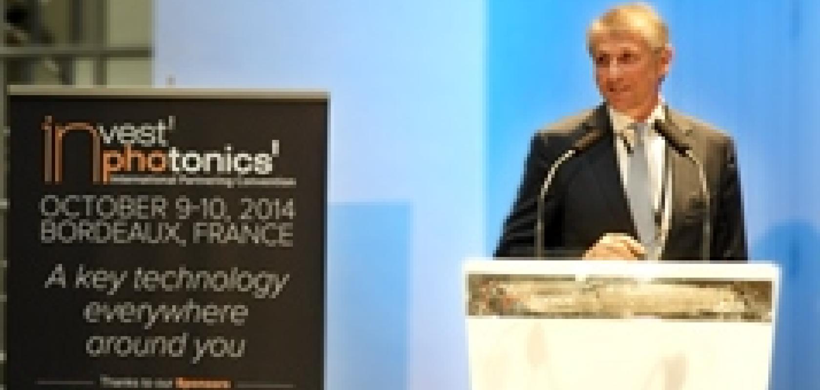
Giorgio Anania, CEO of LED company Aledia and chairman of the conference, recalled in his welcome address how Professor Hiroshi Amano, one of three scientists who won the Nobel Prize in Physics for developing the blue LED, was working with Aledia at the company’s base in Grenoble when he received the news. Professor Amano is a member of the scientific advisory board for Anania, a company developing LEDs based on nanowire technology.
Also speaking at the event, Christoph Thumser, sales director of life sciences research at Leica Microsystems, remarked that Leica Microsystems has worked in close collaboration with Stephan Hell, the Chemistry Nobel Laureate who invented stimulated emission depletion (STED) microscopy. STED is a technique that overcomes the diffraction limit of traditional optical microscopy (around 200nm), offering resolutions of 30nm to 80nm.
Thumser said during his presentation that Leica Microsystems launched its first super-resolution microscopy system in 2004, although this wasn’t a great success commercially. The company then went on to introduce its first STED system in 2007, and Thumser noted that the market for super resolution microscopy is expected to grow by 15 per cent over the next few years, compared to just two to three per cent for the total microscopy market.
The conference attracted 170 attendees bringing together photonics companies with venture capitalists and covering topics ranging from life sciences, electronics, and the environment, to alternative financing. Interspersed with the sessions were pitches from 20 photonic start-ups targeting a cumulative total of €70 million. The pitches were judged by a panel of venture capitalists and investment experts. Since 2008, the event has helped photonics firms raise close to €50 million in funding.
Multinational electronics and internet corporations like Google, Apple, and Samsung are the current big investors in photonics technologies, according to Anania. Speaking to Electro Optics, Anania said: ‘There’s been a real change in who’s financing it [photonics]. The investment is coming from corporate companies rather than venture capitalists. The really big investors are companies like Apple and Google.’
Anania said that Samsung Ventures has a budget of $1.2 billion per year to invest in new technologies, with a typical fund being around $100 million spread over 10 years. This is a huge amount compared to the typical investment from venture capitalists.
Samsung bought OLED company Novaled in 2013 for €260 million and the company’s CEO, Gildas Sorin, was one of the speakers at the event. Sorin commented that photonics technology ‘takes time’ to mature and see a return on investment. Novaled was founded in 2003 and took 10 years to sell. Sorin stated: ‘Innovation will come from start-ups, not corporates,’ adding that there’s money to be made from start-up companies, but it takes time and there will be some risk involved. He said that venture capitalists need courage to make an investment in photonics technology, and that they can’t expect a return on investment in just two years.
George Ugras, general partner at Adams Capital Management, gave the argument from the venture capitalists’ perspective, that technologies like OLED materials that will take 10 years to mature are difficult to fund.
Photonics doesn’t have one large product, Ugras said; there are lots of small companies which makes it difficult for venture capitalists to invest in the technology. The technology has to address a huge market; if it’s not huge, then investment often has to come through government funding.
With venture capitalists being less active, the positive news is that corporate investment is on the rise. ‘I think it’s healthy because these guys [corporate investors] can think medium-term and move technology forward,’ Anania commented.
There are also many growth areas for photonics technologies – Jean-Luc Beylat, president of Alcatel Lucent Bell Labs France, commented that silicon photonics for data centres was a huge opportunity for companies working in this area. According to market analyst, Yole Développement, the silicon photonics device market will grow from $25 million in 2013 to more than $700 million in 2024, at a 38 per cent CAGR.
The ‘elevator pitch’ competition taking place throughout the conference was won by Effect Photonics, a developer of dense wavelength division multiplexing system-on-chip modules that aims to increase the energy efficiency in data centres. James Regan, CEO of Effect Photonics, a 2011 spin-out from the University of Eindhoven in The Netherlands, was presented with the award and the €5,000 prize money.
It is still really difficult for many start-ups to get funding, and the majority of a CEO’s time for these small companies is spent looking for financing. In order to help with this process, the European Photonics Industry Consortium (EPIC) has launched a working group to promote finance activities among its members. Among its first planned initiatives is a photonics venture event in April 2015 to be held in Rome. The event will aim to maximise photonics entrepreneurs’ access to European Commission funding.
Anania commented that there are a lot of positive trends in the photonics industry: ‘The lighting world is going to have a revolution in the next four years… we’re seeing photonics exploding in mobile devices, cars will be packed with photonics. Ten years ago it [photonics] was going into telecoms and the rest was in research labs; now it’s going into a lot of industries.’
