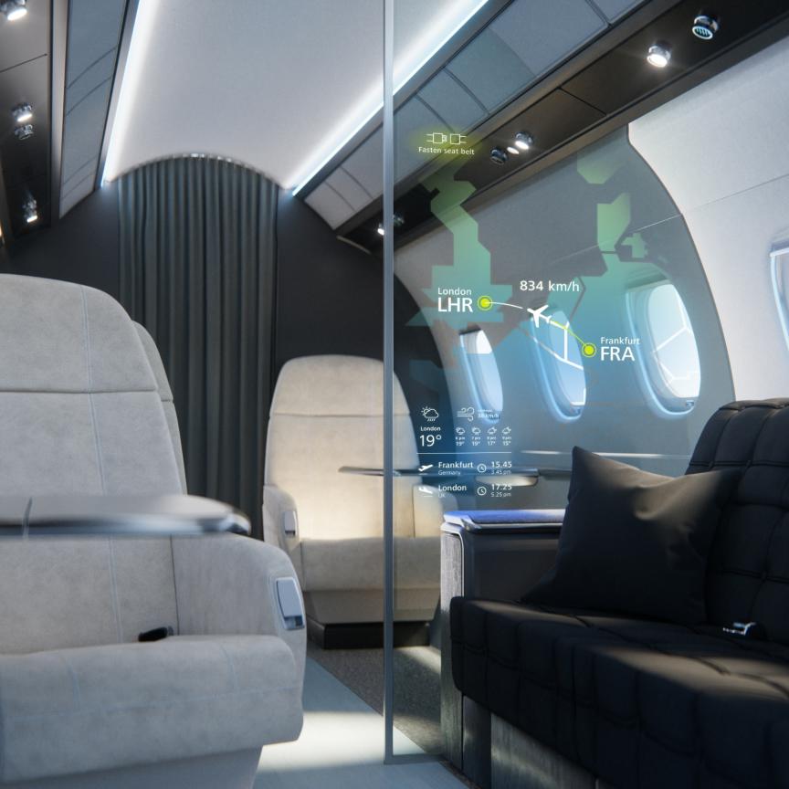
It was less than two years ago, in June 2021, when Mark Zuckerberg outlined his vision for Facebook (now Meta) to lead a new version of the internet – the metaverse.
In this space, the physical world seamlessly merges with augmented, virtual and mixed reality (AR, VR, MR, together referred to as XR) experiences, a space where real and digital representations of people seamlessly interact at work and play.
Although XR goggles have made some inroads into the gaming (e.g. Meta Quest 2, Playstation VR headsets) and business (e.g. Microsoft HoloLens, Varjo XR-3 AR goggles) markets, fast forward to today – when many are predicting a global recession during 2023 – and that vision has lost a lot of its gloss.
“I don’t know if you’ve been living under a rock for the past six months, but just between Facebook, Amazon, Microsoft, Google and Snap, $255 billion has been lost in market cap,” explains Bernard Kress, Director of XR Engineering at Google Labs and recently elected President of SPIE, the international society for optics and photonics. “And these five companies are heavily invested in XR.” In October 2022, Amazon scrapped many of its secret R&D ventures, including its corporate AR headset project. In November, Meta let go of one eighth of its workforce (11,000 employees), many of whom were working on XR hardware. And similar major planned layoffs have been reported elsewhere.
What’s more, it is not just tech giants feeling the squeeze. In Q3 2022, global venture funding dropped by 34%, which is the largest drop in a decade. “During the pandemic, if you raised your hand and said I know how to spell ‘ARVR’ you got $100 million – today is very different,” says Kress. “For example, Leia Inc., a company in lightfield displays, just got $125 million. But it’s not investment, it’s a loan with interest.”
Optics drives
AR/MR Despite this doom and gloom, Kress still sees huge progress being made in XR hardware and, specifically, in what he sees as being key to mass adoption of AR/ MR: wearable, visual and social comfort. How AR/MR glasses feel on a wearer’s head, how a user sees the digital and physical worlds, and how the glasses look are all heavily influenced by the optics technologies under the bonnet.
These technologies can generally be categorised into three key fundamental optical elements that make up AR/MR products: sensing technologies to scan the real environment, a display engine to produce virtual images, and light-directing components to channel light into the eye and produce the virtual images observed by the wearer overlaid onto the environment.

TriLite calibration module algorithms correct the image seen by the eye
All three need, of course, to fit in a small form factor and have low power requirements, which has driven innovators to explore many different approaches. For example, light-directing components – collectively referred to as the ‘optical combiner’ – take the projected image and propagate it along the lens to a suitable area where it is reflected back to the user’s eye, while allowing external light to flood through. Although various types of optical combiner architectures have been explored, waveguide combiners are the only option delivering thin optics with a glasses-like form factor and requisite optimal visual quality for AR/MR.
They consist of an input and output coupler, and a <1mm-thick waveguide between, wherein light is transported through total internal reflection. Waveguide combiners are big business, with tech giants and specialists such as Lumus, WaveOptics and DigiLens vying for prominence. These waveguide combiner products come in a number of different flavours depending on the coupler approach. Reflective waveguides use semireflective mirrors to direct light waves. Polarised waveguides use multilayer coatings and embedded polarised reflectors. Diffractive and holographic waveguides employ deep slanted diffraction gratings and volumetric holographic gratings, respectively. The jury remains out on which approach is best for AR/MR.
Know your surroundings
A similar quandary is seen in sensing technologies for AR/MR. To build a picture of the wearer’s environment in real time, AR/MR headsets can contain a host of different technologies from various companies, including gesture and voice recognition and one or more special types of imaging sensors. These might be timeof-flight (ToF) cameras, vertical-cavity surface-emitting laser (VCSEL) based light detection and ranging (LiDAR), binocular depth sensing, structured-light sensors, or some combination of technologies. “Those modules tend to have not just one but, in many cases, two, three, sometimes up to six 3D sensing modules somewhere within the actual goggles,” explains Metalenz CEO and co-founder Rob Devlin.
Devlin sees metalenses as a potential solution to these complex and costly AR/MR sensing setups. A metalens is a completely flat and planar optic with a nanostructured surface whose scattering properties can be very precisely and finely controlled. Using a metalens, the functions of three or four unique conventional optics can be combined in a single metasurface, as he argues: “If you can replace six modules with, maybe, two metasurface modules, that’s a really big benefit.”
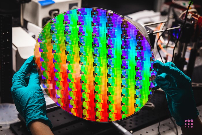
A 12-inch wafer containing ~5000 metaoptics (Image: Metalenz)
Moreover, metalenses could help solve some of the more enduring challenges in AR/MR sensing. “The precision with which we can control light allows us to improve the performance of 3D sensing modules in bright light environments, providing, maybe, a factor-of-two improvement in signal to noise,” says Devlin. This ability would help ensure the experience is the same regardless of whether a user is in a dark room or a sunlit park.
With the company’s first generation of consumer electronics products now on the market, Devlin is already looking to the future. Next-generation products coming from Metalenz will use metalenses to shrink tabletop sensing devices such as polarisation cameras, which have never been incorporated in mobile devices before: “When we can start to bring entirely new information sets that people or machine learning algorithms haven’t been able to access, it’s almost like you’ve given people another sense – that’s the really exciting aspect of all of this,” he says.
Scanning an image of the metaverse
Much like optical combiners and sensing technologies, the right approach to building AR/MR display engines has not been settled either. A display engine projects virtual images onto a small peripheral area of the display lens. For this, a slew of approaches including microOLED (micro organic light-emitting diode), LCD (liquid crystal display), LCoS (liquid crystal on silicon), microLED (micro light-emitting diode), DLP (digital light processing) and LBS (laser beam scanning) are being explored, all at different technology readiness levels, and each with advantages and disadvantages when it comes to their potential to deliver efficient, small, bright and light displays with high resolution and large field of view.
Founded in 2011, Austrian technology company TriLite has bet the house on LBS. Co-founder and CTO Jörg Reitterer explains why. “Common display architectures today consist of panel-based displays; essentially 2D arrays of many, many pixels,” he says. “For a given resolution or for a given field of view, we see this as a fundamental limitation of how small you can make the system because at some point you cannot make the pixels any smaller and the panel just has a certain extension.”
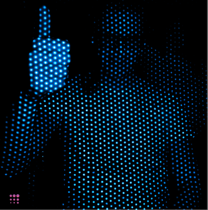
Example of dot projection produced by Metalenz metaoptics. (Image: Metalenz)
What’s more, Reitterer says that displays such as LCoS and DLP require illumination optics to deliver light to the panel, adding complexity and bulk to the system. In contrast, microLED and microOLED are self-emissive, but still require additional projection optics in front of the panel to collect the light and inject it into a waveguide.
“Another key issue is with yields,” Reitterer adds. “If you have many, many millions of microLEDs, for example, on one common substrate, you need to make sure that all of them are working, which becomes very, very tricky.” Reitterer argues that LBS has none of these disadvantages, making it the best overall architecture to provide the necessary performance, flexibility and scalability to meet the demands of the AR/MR market.
LBS does away with both a panel and projection optics, and instead relies on tiny microelectromechanical systems (MEMS) mirrors that can rotate to scan the laser pixels across a given field of view and through a per-pixel modulation schema. Unlike LBS competitors, the Trixel 3 has a single 2D MEMS mirror with no relay optics. This pared-back setup ensures that the image that goes into the eye is perfect – no extreme lens tolerances, fiddly alignment or additional optics are required.

Mockup of Trixel 3 installed in smart glasses (Image:TriLite)
TriLite has built the world’s smallest projection display based on LBS technology. The Trixel 3 weighs 1.5g and is less than 1cm3 by volume, meaning it can fit unobtrusively in the side of a pair of smart glasses. The company achieved such miniaturisation by shifting complexity from the optics hardware to the software. This software includes fully automated calibration and correction setups with machine learning, and laser pulse timing algorithms that eliminate image distortions by enabling perfect overlapping of RGB colour channels. “This is something that we see as a big USP for LBS in general and especially for our systems,” Reitterer adds.
Having built partnerships with leading MEMS mirror developers including Infineon and waveguide suppliers such as Dispelix, TriLite has ensured that the Trixel 3 is compatible with market-leading AR hardware. With the company releasing evaluation kits to the market in early 2023, it seems likely the Trixel 3 display engine will be powering commercial AR/MR glasses soon.
Display engine of the future?
But others in the industry feel microLEDs hold the most promise as display engines. “For technologies such as laser beam scanning, the problem is that the lasers use a lot of energy,” says Applied Materials VP Nag Patibandla. “A very high resolution, very bright display that can run in an energy efficient manner means it has to be self-emitting – and we think the primary option for this is gallium nitride-based microLEDs as the light emitting devices in the display.” Applied Materials is a globally leading provider of equipment for manufacturing chips and displays, and a pioneer in developing optical components for the XR industry. It too recognised the microLED yields issue early on.
“The obvious way to build a microLED display is to take a green emitter, blue emitter and red emitter from three different source wafers and transfer them onto the backplane that contains three subpixels, repeating three times, which becomes exponentially difficult without damaging the ones that are already there,” explains Patibandla. “Instead, we take UV LEDs, transfer them from a single-source wafer in one transfer step, and then, with a very high-resolution printer, print and cure red, then green, then blue quantum dots on top of each LED die.”
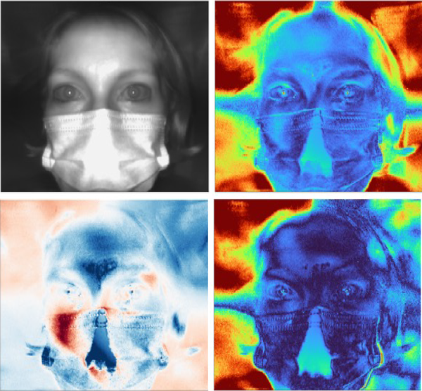
PolarEyes captures all polarisation information, making ultra-secure biometric authentication possible in an extremely small module (Image: MetaLenz)
Already, Applied Materials has used this technique to build a smartwatch-sized microLED display. However, this is far from what is required for commercial AR/MR display engines. “There are two numbers I keep telling my engineers to remember: 1 million nits and 10,000 ppi,” says Patibandla. A million nits (a nit is a unit to gauge how bright a screen appears to the human eye) is more than 2,000 times brighter than a typical phone screen, but is necessary as the internal optics in AR/MR systems run at 1 to 2% efficiency. Equally, 10,000 ppi (pixels per inch) is at least 16 times higher resolution than a smartphone, but is needed to remove the ‘screen door effect’ that makes AR/MR users feel like they are viewing the world through a mesh.
“We are still at 1,600–3,200 ppi resolution with our approach right now,” says Patibandla. “When you start including emitters at the 1 micron range, and you’re trying to get visible light at wavelengths of 450–630nm, you don’t have sufficient paths for minority carriers to emit photons before they see a defect and disappear – so to get to 10,000 ppi, we need to solve a basic physics problem.” As a result, mass-produced RGB microLED display engines for XR displays remain a technology for the future.
As with any nascent technology, it is unclear how long it will take innovators to make the breakthroughs needed and hit upon the right combination of tools that make AR/MR commercially appealing to the masses. But with XR’s potential to enhance how we work, rest and play, the safe bet is that time will be sooner rather than later.
The challenges of manufacturing high-volume freeform optics
Freeform optics have been available since the 1970’s; however, they were typically restricted to highly specialised applications because of the high cost due to technical and manufacturing limitations. In recent times, freeform optics have been utilised in low-volume imaging applications for R&D, aerospace, and government-supported projects.
The benefits of implementing freeform optics are clear. They allow for custom aberration correction, redistribution of optical/mechanical tolerances, and even allow for a reduction in component count and system volume. These benefits are achievable because each freeform optic is uniquely designed around each system’s requirements. The design freedom allowed provides many options to optimise an optical system, enabling a more compact instrument. However, the high cost of freeform optics, until now, has constrained widespread, high-volume commercial adoption.
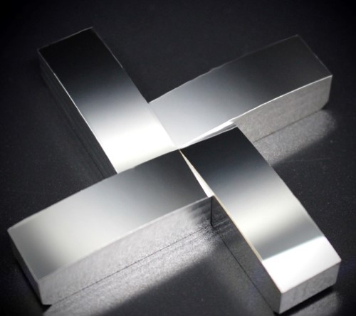
Figure 1: Freeform mirrors manufactured by Spectrum Scientific
When it comes to the available high-volume manufacturing methods, the choice is between direct manufacturing of original components (using methods including diamond turning, grinding and polishing, MRF, and hand-figured), moulded optics (both injection and glass moulding), nickel electroforming, and optical replication.
Direct manufacturing methods are expensive options where each component is usually produced one at a time, requiring many hours of operation to produce a single part. While these processes allow for a wide range of flexibility, long lead times and high costs make direct manufacturing unfeasible from both a cost and time perspective for high-volume imaging applications.
High-volume production is feasible for plastic injection and nickel electroform from a cost perspective and both methods can reduce the variability between batches. However, these methods offer less flexibility due to material choices, size and optical surface quality limitations, making them unsuitable for demanding imaging applications.
The optical replication process used by Spectrum Scientific provides the only viable alternative to these traditional manufacturing techniques. Optical replication is an established manufacturing process that has been around since the late 1960s. The process works by transferring the optical surface of one original or master optical surface onto other surfaces, thus creating copies of the original. Using this process, the profile of the original optic is faithfully preserved and transferred, producing a replicated optic that’s virtually indistinguishable in performance from the original master, with excellent reflected wavefront and low surface scatter. This process is repeated numerous times to support volume requirements. As each The challenges of manufacturing high-volume freeform optics replicated optic is almost identical to the original optic, there is a high degree of batch-to-batch repeatability.
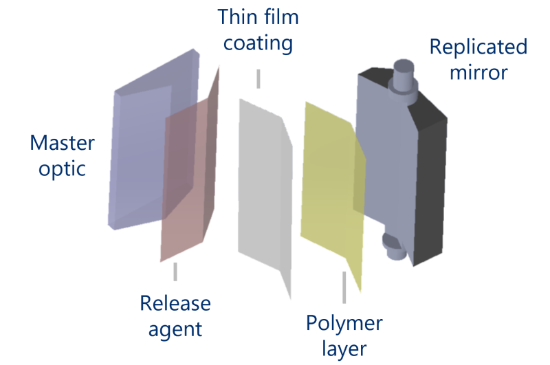
Figure 2: The optical replication process
In addition, the substrate can be machined with additional alignment mounting and registration features directly onto the replica substrate, reducing the number of parts, decreasing the assembly time and likelihood of ongoing maintenance costs. By choosing a substrate with a low or high coefficient of thermal expansion, a thermalised design is also enabled.
Spectrum Scientific has used optical replication for manufacturing high volume holographic gratings, aspheric mirrors, and hollow retroreflectors since 2004, and in 2018 extended this manufacturing capability to produce high-volume, low-cost freeform optics with aspherical profiles to exacting specifications, offering significant benefits and cost-savings for today’s optical systems.
One key benefit of the optical replication process is the ability to quickly ramp up production without incurring additional capital equipment costs, which offers a significant advantage for complex optics such as freeform mirrors. This was demonstrated when Spectrum Scientific had to quickly increase monthly production of a complex freeform mirror for a major customer from 500 units a month to more than 1,200 units per month over a six-month period to meet end-user demand. This was achieved smoothly and with no additional manufacturing investment required.
One of the challenges of the design, manufacturing, and measurement of a freeform mirror is effective communication and interpretation of the optical surface. Generalised asphere equations that have been modified with either polar or cartesian forms, Zernike polynomials, and other implicit polynomial methods are often used to describe the freeform surface. Spectrum Scientific generates a SAG table which is verified by the customer to ensure the optical surface is correct, resulting in a freeform mirror that meets the customer’s needs.
Typical specifications that can be met using the optical replication process include:
- Aluminium or glass substrates
- From 0.5-inch diameter
- Surface figure down to λ/10 or better
- Surface roughness down to 3.5Å
- Broadband metal or dielectric coatings from 120nm to 10μm
Further information: www.ssioptics.com