Even as TV viewers are touched by experiences as intense as falling into the black hole in the movie Interstellar, they likely think viewing can’t get much better. Given the current display technology, can companies keep improving optoelectronic technologies in a way that consumers will appreciate? Does anyone really want even wider colour gamut, or to progress from the amazing resolution of today’s 4,000 pixel-width 4K displays, on to the successor 8K? Perhaps they will, when they see the truly remarkable advances in display quality and even glasses-free 3D effects that companies are developing.
TVs are already evolving to the point where they will all be 4K, said Raghu Das, CEO of market analysts IDTechEx, based in Cambridge, UK. ‘It will take a number of years, since it will be driven by the amount of 4K content, but when people come to renew their TV they often go for the best technology,’ Das said. Improving resolution is a noticeable benefit, he explained. ‘Often people see TV as a long-term investment and therefore tend to buy the best at the time that their budget will afford for future-proofing.’ Among the many technologies helping drive higher resolution, Das highlighted organic light emitting diodes (OLEDs), quantum dot displays, and microLEDs.
Both OLEDs and microLEDs are ‘emissive technologies’ creating pictures from arrays of shining LED pixels. This differs from the best-established liquid crystal displays (LCDs), where the images formed must be illuminated by emission from behind by a backlight, typically an LED-powered one today. However OLEDs’ brightness and efficiency in turning electricity into light are limited. MicroLEDs bring the possibility of high-resolution emissive displays with the high efficiencies typical of LEDs, because microLEDs are 20 x 20µm compared to 200 x 200µm for LEDs. MicroLED prototypes have already demonstrated power consumption as low as 10 per cent that of an LCD display and half that of an OLED panel.
But making microLED displays is difficult. GaN microLED chips must be separated from the sapphire crystals they’re deposited on, and assembled onto a display backplane. A 4K display requires nearly 24 million microLEDs, which would take six weeks to transfer using pick-and-place methods. Santa Clara, California-headquartered Coherent therefore supplies its UVBlade lift-off tool as a high-speed solution, explained Ralph Delmdahl, product marketing manager. Processed micro-LED epi-wafers can be bonded to temporary carrier wafers using UV absorbing polymer adhesive films. The UVBlade’s 248nm excimer laser vaporises the adhesive, detaching the microLED chips and putting them on the backplane panel, assembling a 4K display in less than a minute.
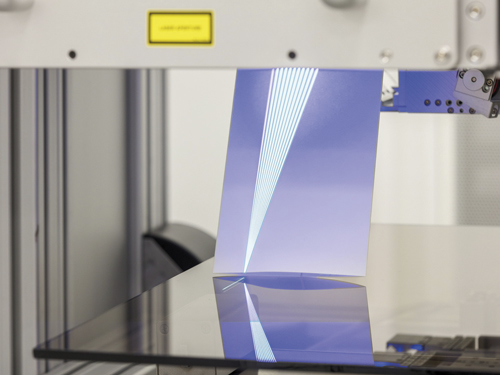
The UVBlade line beam system for wafer based lift-off processing. Credit: Coherent
‘Demand for UVBlade lift-off tools adapted for LED wafer processing is starting to emerge, in line with the growing microLED market, though the latter is far from mature yet,’ said Delmdahl. A key challenge for microLED makers is getting a high enough yield of fault-free displays. Delmdahl said that UVBlade helps with this through its gentle lift-off process, enabled by homogeneous energy distribution and stable beam and energy density.
Flexible solutions
UVBlade’s potential in microLED manufacturing builds on its usage for laser lift-off in OLED displays, where it helps produce devices on flexible backplanes. Delmdahl highlighted the 77-inch wide, transparent, flexible OLED screen demonstrated at the DisplayWeek conference in Los Angeles, California, in 2018. ‘Technically, and also economically, lift-off separating such large displays from their giant motherglass panels requires record line lengths of 1,200mm,’ Delmdahl said. ‘Coherent is the only company which has realised, shipped and installed a 1,200mm line-length UVBlade system to support the flexible OLED TV market.’
This illustrates how OLED technology is shifting from displays on glass to rigid plastic, which is thinner, more robust, and can be curved or fully flexible, Das highlighted. ‘This may prove a big boost in turning round the flatlining, or declining, tablet and smartphone market and allowing display makers to capture more profit margins, since it is not yet a commodity,’ Das said.
Such continued innovations are largely being pushed by suppliers, Das observed. ‘Margins on LCDs have fallen due to competition from Chinese-based panel makers,’ he said. ‘It’s innovate or die – as many Japanese companies have learnt. Huge LCD investment in China meant those in Korea and Japan lost margin and ended up, in some cases, leaving the display business. It resulted in huge innovation in OLEDs. Chinese display makers are also hot on OLEDs and other technology, and will be quite formidable competition, but for now the Koreans are in the lead.’
Such innovation is slowly improving OLED for TV’s biggest problem today, which is cost, Das added. ‘Printing potentially promises very large area displays beyond the current panel sizes today, restricted by conventional non-printing processes,’ he said.
One leading OLED printing player is Newark, California-headquartered inkjet tool producer Kateeva. Inkjet printing is already used to deposit and pattern a key encapsulation layer in OLED smartphones, explained Steven Van Slyke, Kateeva’s chief technology officer. ‘All the flexible and foldable smartphones in existence use this technology, and Kateeva has provided essentially all of these tools,’ he said. ‘It is expected that this same technology will be used for TV-sized displays in the future.’
OLED manufacturers are also inkjet printing the emitters in red-green-blue (RGB) full colour displays. That differs from the white-red-green-blue (WRGB) format, which relies on combining an unpatterned white emitter with colour filters to produce the red, green and blue. Kateeva has demonstrated inkjet printing for 210 pixel per inch (ppi) RGB displays. ‘A 55-inch TV with 8K resolution is about 160ppi,’ Van Slyke underlined. Kateeva is providing R&D tools to China and Korea for RGB printing development to enable ‘top emitting’ OLEDs, in which the emitters are in front of their control circuitry.
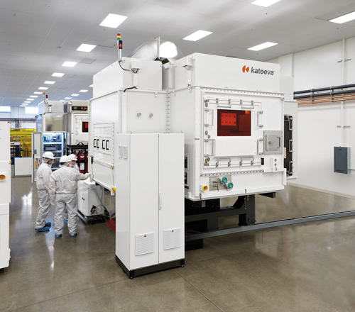
Kateeva’s YieldJet Flex system for OLED thin film encapsulation. Credit: Kateeva
Top emission fits RGB formats better, partly because WRGB colour filters cause issues. They must either be patterned on top of the OLEDs’ encapsulation layers, or on a separate piece of glass aligned and laminated to the OLED substrate, Van Slyke explained. The latter is an undesirable additional process step and use of materials. Also, top-emitting OLEDs create micro-cavities in their material stack, between their semi-transparent top cathode and reflective anode. This cavity’s optical properties favour wavelength ranges that mean pure white emission is not feasible. With inkjet printed RGB displays, each pixel’s colour can be designed to take advantage of the micro-cavity, Van Slyke said.
Quantum leap
Inkjet printing is also helping enhance both OLED and LCD technology using quantum dot colour filters (QDCFs). Such filters could sit in front of a blue LED-based backlight, with an LCD modulating the blue light reaching the QD film, Van Slyke said. Alternatively, Samsung is developing a blue OLED backplane directing the light to the appropriate pixelated QD film. ‘In this case, the blue OLED emitter is unpatterned, so it is scaleable to large mother glasses,’ Van Slyke said. ‘Likewise, the QDCF layer deposition by inkjet printing is also scaleable to large substrate areas. This approach is receiving much attention recently, and is in the advanced development stage. So far, it looks promising as a competitive display technology.’
Abishek Srivastava, from the Hong Kong University of Science and Technology (HKUST) and his colleagues are working on similar quantum dot enhancement film technology. Rather than quantum dots, HKUST is developing quantum rod-based films, aligning them with liquid crystal molecules, giving polarised emission. This doubles emission efficiency from around 4 to 8 per cent, Srivastava explained, and spans wider colour space. Whereas the commercial cutting edge for colour is around 90 per cent of the recommended specifications known as BT.2020, the HKUST team achieved 96 per cent. ‘I think that’s the best case reported for any LCD until now,’ Srivastava underlined.
LCD producers have been improving display parameters continuously, Das stressed. A good example is in one of their previous biggest shortcomings, viewing angles, which have improved steadily over the last 15 years. With market shares declining, remaining LCD producers are looking to eke out such benefits for as long as possible, he added. One innovation is making LCDs flexible, as the company FlexEnable is doing. ‘Large LCDs for TVs will be here for some time, small displays are more rapidly moving to OLED,’ he pointed out.
HKUST has been working with Hsinchu, Taiwan-headquartered display giant AU Optronics (AUO) on another potential LCD innovation. Field sequential colour (FSC) eliminates colour filters, which take up space and absorb 70 per cent of the output from the backlight. Removing them therefore makes LCDs more energy efficient. FSC rapidly shows different colour images sequentially, relying on human vision to fuse them into a full-colour picture. FSC displays can therefore ‘have three times higher resolution’, Srivastava said, because only the desired pixel colour emits light, rather than the entire display backlight. However, FSCs need low driving voltages, and very fast electrical field responses.
Ferroelectric liquid crystals (FLCDs) meet the driving voltage and electro-optical response requirements needed for FSCs, Srivastava explained. FLCDs were invented in 1975, but until now they have been very sensitive to mechanical shock. ‘If you touch the screen, the optical contrast drops straight away,’ Srivastava said. HKUST scientists discovered that the ferroelectric liquid crystal material’s elastic energy was not previously balanced with the anchoring energy of the alignment layer needed to orient the liquid crystals. They have developed new materials that improve that energy balance, enabling very high contrasts and robustness against mechanical shocks.
Another dimension
Among the best LCD technologies today is the low-cost, two domain in-plane switching (IPS) used in Apple devices, Srivastava said, offering much better viewing angles than conventional LCDs. FLCDs should be better still, he added, and also outperform OLED. ‘OLED or any other kind of display needs subpixels to show full colour images,’ Srivastava explained. ‘But field sequential displays only need one pixel to show three colours, and because this requires very small driving voltages, we can go up to 2,000ppi resolution without problems. We’re trying to make 2,500ppi.’ The team’s partner company is evaluating the technology’s commercial use, Srivastava added. That might seem excessive, but high resolutions will help attempts to bring displays into the third dimension.
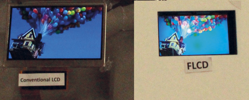
FLCD field-sequential displays enable a wider colour range than existing LCD technologies. Credit: Hong Kong Institute of Science and Technologies
Dimenco, based in Veldhoven, Netherlands, produces glasses-free 3D displays by applying a lenticular lens on top of a display, explained Huub Van Kuringen, process development engineer at Dimenco. ‘The lenticular lens divides the pixels over the eyes of the user, which creates a 3D perception,’ she explained. ‘An eye-tracker is used to see the best 3D from all positions, and with current high-resolution displays, the resolution for both eyes is good as well. For our 2D-3D switchable displays we use liquid crystals, which can turn the lenticular lens on and off.’
Such approaches have been explored since the 1990s, but suffered from crosstalk between component images being shown to viewers. The issue arises in the polyimide (PI) alignment layers. ‘PI is a well-performing alignment material on planar surfaces,’ Van Kuringen explained. ‘But on non-planar surfaces, such as lenticular lenses, the PI layer deteriorates the optical quality of the lens structure. This results in cross-talk ghost-images. Recently, we have replaced the PI layer of the lenticular lens with nano-grooves. These nano-grooves align the liquid crystals very well. Thanks to the small dimensions and irregularity of the nano-grooves, they do not scatter light or cause interference, and the optical quality of the lens has been improved significantly.’ Dimenco reduces crosstalk to less than one per cent, for a ‘natural and pleasant viewing experience’.
In principle, any 2D display can be used to make a 3D display, explained Silvino Presa, head of optics at Dimenco. ‘However, not all of them will result in the same quality,’ he added. ‘High resolution displays are better, because the bonding of the lens will reduce the number of pixels. Our switchable lenses work with linearly polarised light, which is emitted by all LCDs and also some other display technologies.’
Such advances show how, across all display technologies, intense competition for consumer spending is driving optical innovation. In what could be considered a case of ‘survival of the prettiest’, the resulting visual delights will be valued by all but the most cynical viewers.
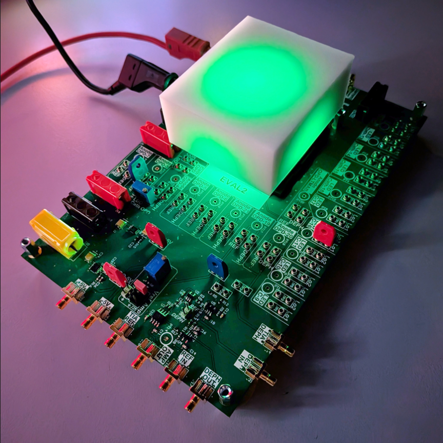
Top image: Dimenco incorporates 3D display technology into Simulated Reality, which it calls a natural user experience, interacting with 3D objects in a virtual environment, without the need of any headwear or wearables. Credit: Kateeva