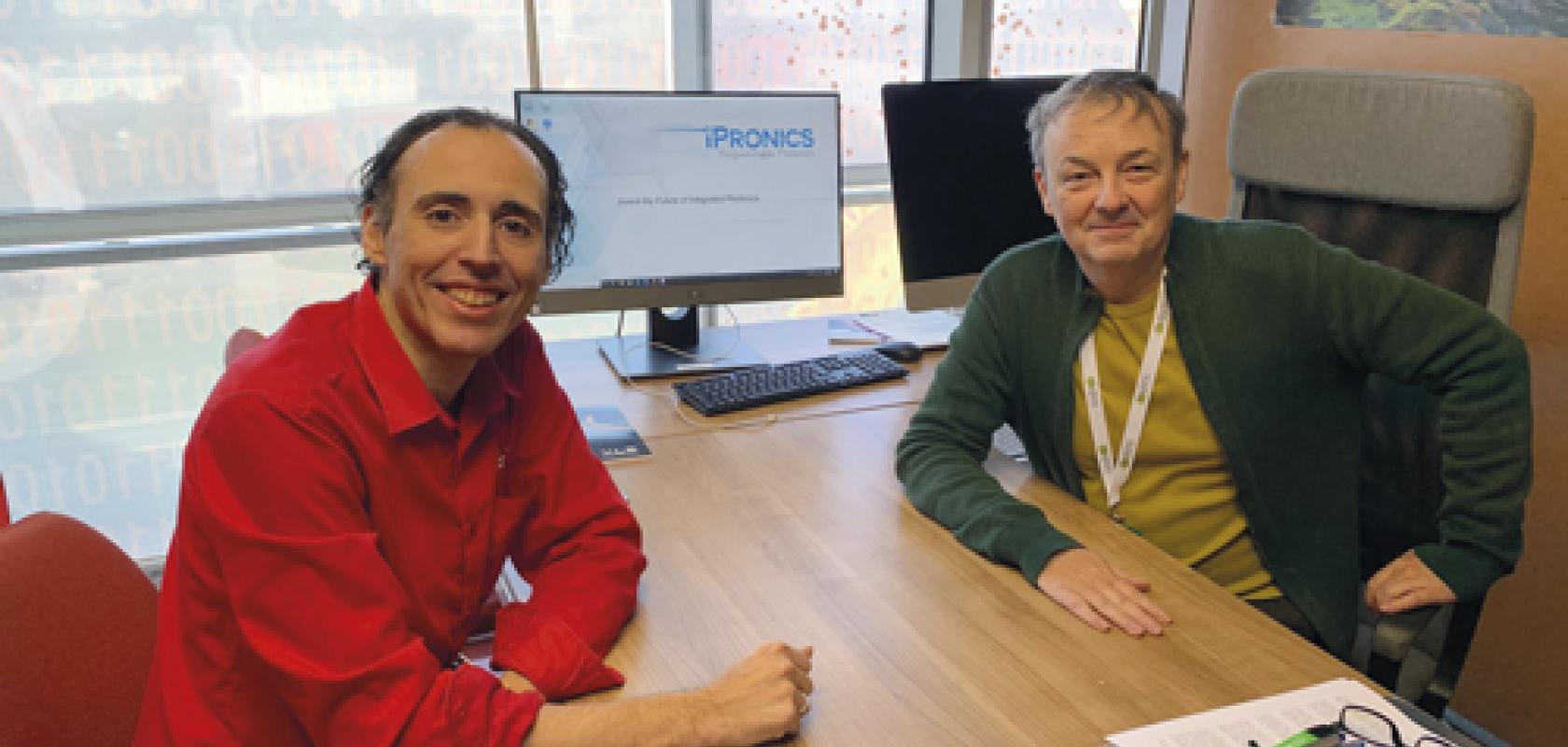
What’s the background to your involvement with iPronics?
After completing a PhD in Telecommunications Engineering at the University Polytechnic of Madrid in 1991, I went into academia and supervised a small research group developing new research lines, mainly in radio frequency (RF) photonics.
In 2000, we started to expand and got involved in a number of European projects. I realised that I needed to know more about physics. So, in 2005, I enrolled in a second distance-learning degree in physics, followed by a second PhD on sub-carrier multiplex quantum key distribution.
We then got a large grant from the Spanish government to do a research project on multiplex quantum key distribution. The project was built around a large team based at the Institute of Photonic Sciences (ICFO) in Barcelona. Although we got some nice results, in 2011, the funding dried up and we had to concentrate on other activities for which we had funding. These mainly focused on radio-, fibre-, and micro-photonics.
During this period, I became interested in the knotty problem of integrated micro-photonics design: sometimes devices worked, sometimes they didn’t. We came up with the idea of trying to create something with a degree of flexibility – something generic that would perform a similar role to the transistor in electronics. We thought about doing reverse engineering and creating an open oscillator, a type of RF photonic transistor. Then we saw the possibility of including extra devices in the photonic segment. We started with very simple filters, then made it more complex by switching connections between the filters. We wanted to create something generic, rather than specific and importantly, something that could be programmed. We started to program the devices and each time got closer to what we wanted – finally demonstrating the feasibility of programing photonics.
Having proved the technology, how did you come up with the idea of iPronics?
In 2015, I began to supervise a PhD student who was researching programmable photonics and two years later I took him on as a post-doc to research programmable RF integrated circuits.
We began to think about how we could extend the concept by switching the connections between filters, and expand the technology into broader areas that had industrial and commercial applications.
The aim would be to provide field programmable photonic gate arrays (FPPGAs), based on a generic, software-defined optical hardware capable of performing multiple tasks.
In late 2017, we started to think about the project more seriously. We brought in other colleagues from the group and finally launched the company in early 2019. We decided to create it as a spin-off from the university, and to become a member of EPIC, of course!
Do you intend to address today’s problems like 5G or IoT, or the problems of tomorrow, such as quantum computing?
Our ultimate goal is to make a device that has a specific set of elements, but which is flexible enough to provide a wide variety of configuration possibilities, for today’s needs and tomorrow’s. Remember that in the telecoms industry no one has been able to predict the future and, in fact, most predictions have been wrong. In integrated electronics, for example, the FPGA was never conceived as an integral part of transceivers but nowadays, transceivers are the main market for FPGAs. Our roadmap makes provision for the same type of evolution, because we know that the design used in the architecture for the first prototypes will need to adapt to meet the new applications requirements and functionalities of tomorrow.
You aim to enter the market in 2021. What supply chain will you need in the next two years?
We’ll need three different tiers. Tier 1 will be for pure photonic integrated circuits and we’ll need good foundries and packaging services. Tier 2 will be for the electronics: there will be issues concerning controlling optical signals and of power for controlling light. There will also be challenges in integrating the electronics and photonics, which are not likely to be resolved quickly. Tier 3 suppliers will be software firms, and this is the most important part to get right. Software is where added value lies. It will have to comply with both electronics and photonics and deal with multi-task operations. The user will need to control and monitor the chip and solve problems, such as finding the optimal placement of circuits, manually or automatically. A lot of elements will need to be controlled simultaneously and there will be challenges in reducing losses and power consumption. To do this, the normal approach of controlling one element will not suffice. A different way of tackling the problem is required, such as using algorithms to tackle collective issues and possibly machine learning techniques for optimisation.
If you could start again, what would you do differently?
Some training abroad to get cross-cultural influences and learn about different approaches and philosophies.
What advice do you have for young entrepreneurs?
I’ve always been blessed by being surrounded by talented people. It’s crucial to take care of the people you are working with, even more than for yourself, because they are the future. What I always try to get into people’s minds is it should never be about one person – it’s a philosophy. You’re not going to be here forever. When you retire, make sure you leave a strong team behind.


