A research project led by the Fraunhofer Institute for Solar Energy Systems (ISE) has developed a proof of concept for a silicon solar cell production line with a throughput of 15,000 to 20,000 wafers per hour.
This represents double the usual throughput and is due to improvements to several individual process steps. The concept was presented at the World Conference on Photovoltaic Energy Conversion in Milan at the end of September.
The research project is being funded by the Federal Ministry for Economic Affairs and Climate Action and involves plant manufacturers, metrology companies and research institutions.
‘In 2021, 78 per cent of all silicon solar cells were produced in China,’ explains Ralf Preu, Division Director of PV Production Technology at Fraunhofer ISE. ‘In order to deploy more solar installations as quickly as possible and to make our supply chains more robust, Europe should re-establish its own production centres for high-efficiency solar cells.’
Preu continued: ‘By boosting throughput and making production technology more resource-efficient, we can cut costs considerably and unlock sustainability potential that we will be able to leverage thanks to process knowledge and engineering excellence.’
New concepts for silicon solar cell production
The consortium investigated every stage of the production of high-efficiency silicon solar cells to optimise the entire process. Several process steps required new developments.
‘For some processes, established production workflows needed to be accelerated, other processes needed to be reinvented from scratch,’ explains Dr Florian Clement, project manager at Fraunhofer ISE. ‘Compared to the numbers we currently see, the production systems developed within the scope of the project achieve at least double the throughput.’
One of the new developments saw the researchers implement new on-the-fly laser equipment which continually processes the wafers as they move at high speed under the laser scanner. For the metallisation of solar cells, the consortium introduced rotary screen printing instead of the current standard process, flatbed screen printing.
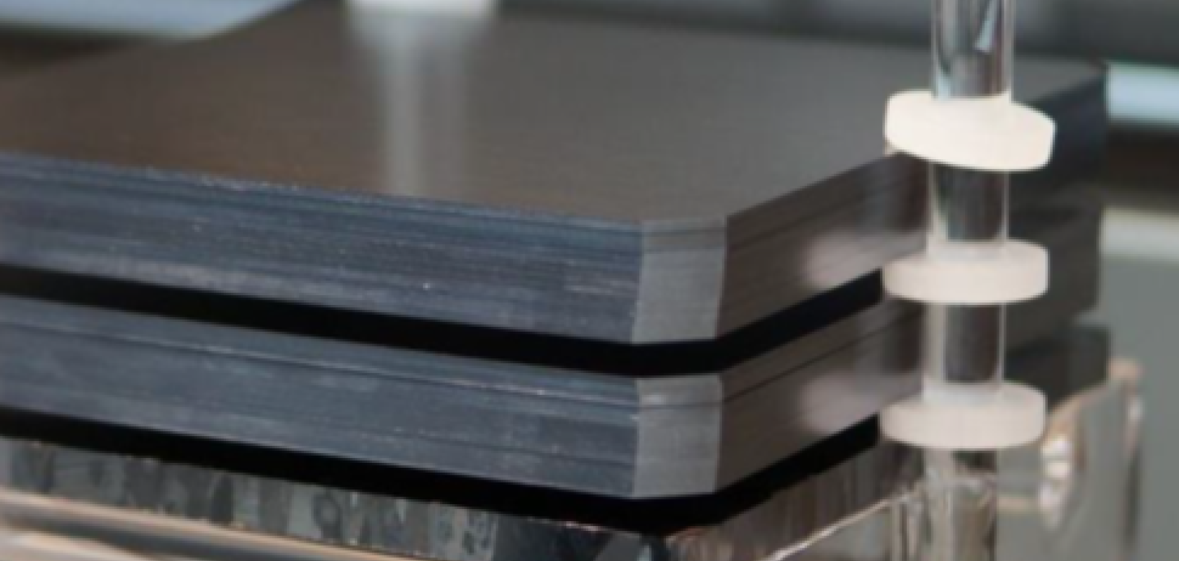
Solar cells require differently doped sections, for example where silicon layer and metal contacts meet. The Fraunhofer ISE researchers integrated the diffusion process used in this context and the thermal oxidation of the wafers into one process step. Wafers are no longer placed individually but stacked on top of each other to be processed in the furnace. As a result, the oxidation process creates the final doping profile and achieves surface passivation at the same time increasing the throughput of the process by a factor of 2.4.
Faster inline furnace processes
Following the electrode imprint on the solar cells, the contact of the electrodes to the silicon solar cell is formed on both sides in inline furnaces. Standard furnaces would have required a significantly larger heating chamber to increase throughput at this stage. Instead, the project consortium installed a three times faster belt speed in the furnace and compared the quality of the sintered solar cells with today’s standard. They were able to significantly increase throughput while not compromising the efficiency of the solar cells.
Contactless testing and analysis of defects
For the characterisation of the complete solar cells, the consortium devised two concepts. A contactless method and a method using sliding contacts were implemented to enable future production lines to test cells faster. This makes it possible to keep up a continuous speed of 1.9 metres per second while measuring the cells, with the team demonstrating great measurement accuracy for both concepts. A patent has been filed for the contactless method.
