Engineers from the University of California San Diego and the PIXAPP European packaging pilot line are developing an educational toolkit to bring integrated photonics into earlier stages of the science and engineering curriculum.
The toolkit is designed to teach undergraduates practical skills in integrated photonics, including how to characterise and test photonics integrated circuits – skills that are typically only acquired at PhD level. The team envisions that teaching these skills earlier on will enable more graduates to enter the integrated photonics industry workforce and meet the growing demand for photonics technicians and engineers.
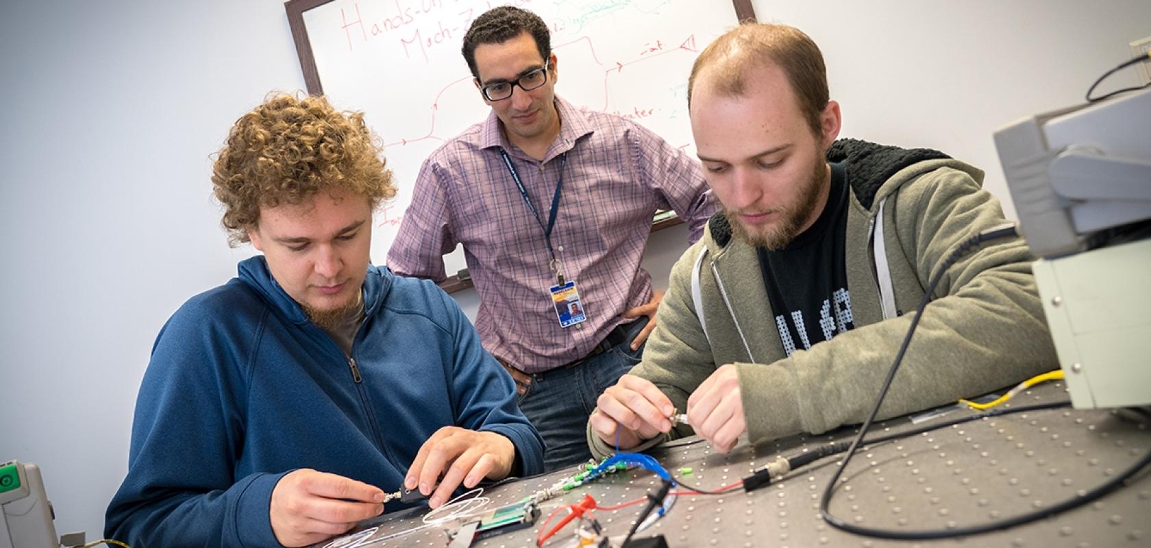
The project was initiated by Abdelkrim El Amili, a research scientist in the Department of Electrical and Computer Engineering at UC San Diego. The UC San Diego team is collaborating with researchers led by Professor Peter O’Brien at the Tyndall Institute in Cork, Ireland, and director of the PIXAPP pilot line.
The team is presenting a prototype of the toolkit at the 2019 Optical Fiber Communications Conference and Exhibition (OFC), which is taking place this week in San Diego.
‘This toolkit will bridge the gap between the growing demand in the silicon photonics job market and the supply of technicians and engineers who have practical skills in the field,’ said El Amili.
‘As the market grows, there will not be enough graduates to fill all these opportunities because only PhD graduates so far have the practical skills in integrated photonics,' he added. 'But learning integrated circuit design, device fabrication, packaging and testing should not be limited to PhD students. Our hope is that by bringing hands-on integrated photonics training to undergraduate and Master’s students, this toolkit will equip them with the knowledge and skills to fill new job opportunities.'
The toolkit, dubbed Integrated Photonics Education Kit (IPEK), is a packaged silicon photonic platform. Instructors can use it as part of an engineering laboratory course to teach students basic building blocks of photonics integrated circuits. By experimenting and tinkering with the plug and play kit, students can gain experience designing, assembling and testing photonics integrated circuits.
The current prototype includes photonic components such as a waveguide, micro-ring resonator, short and long Bragg mirrors, filters, and a Mach-Zehnder interferometer. These are basic building blocks in educational, research, and industrial environments. Many of the devices are electrically tunable to demonstrate various modes of operation to the user, and can also combined together externally using fibre for more complex photonic functionality.
IPEK offers many of the functionalities of conventional photonics platforms for a reduced cost of around $1,500 to build, in comparison to a conventional setup costs around $10,000 to $12,000. And while conventional platforms are bulky and require a separate lab space, IPEK is portable - the current prototype fits in a user’s hand.
IPEK is also robust and easy to use, said El Amili. With the plug and play package tool, users no longer need to spend time aligning and stabilizing the optical fibre like they would with a conventional platform. 'We gain time in performing the experiment,' he said.
'Tyndall and PIXAPP recognise the need for a skilled workforce in integrated photonics across all skill levels. The IPEK toolkit is an excellent initiative dedicated to training the next generation of engineers and technicians,' added Tyndall's O’Brien.
The international team is now working to refine the prototype, while El Amili and colleagues are preparing a laboratory curriculum at the UC San Diego Jacobs School of Engineering to implement the toolkit.
Image: Abdelkrim El Amili (centre) is leading a project at UC San Diego to develop an educational toolkit to teach students practical skills in integrated photonics. Credit: David Baillot/UC San Diego Jacobs School of Engineering