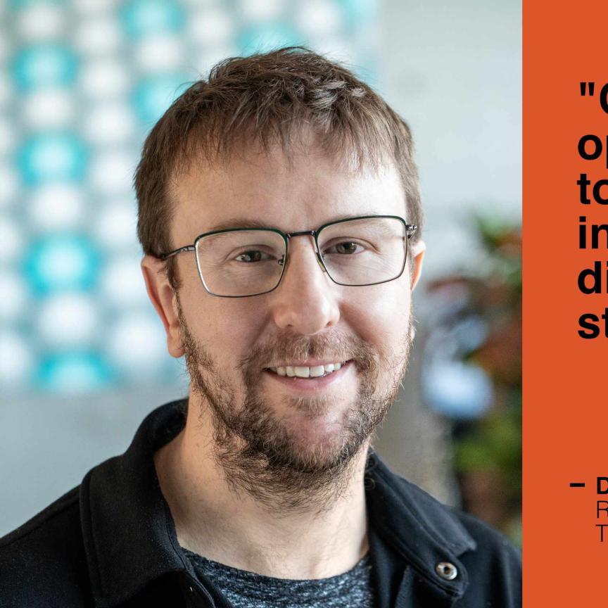
Attolight and CEA-Leti have entered into a joint-development programme to apply Attolight’s cathodoluminescence microscopy to semiconductor materials.
Attolight’s combination of electron and light microscopy reveals ultra-trace impurities and crystallographic defects not visible using other imaging techniques. The company’s core expertise is a measurement technique called cathodoluminescence, a non-destructive characterisation method yielding a level of data that provides a deeper understanding of material structures and properties. The programme with Leti is designed to extend the technology for use in the chip industry and research applications.
'This joint-development programme with CEA-Leti is a major milestone for Attolight. It is a clear indicator of the value of Attolight’s innovative technology for research in a variety of applications,' said Attolight CEO Samuel Sonderegger. 'We are very proud to collaborate with such a prestigious partner and this development clearly endorses the quality of Attolight’s products.'
'Our integrated cathodoluminescence approach opens new areas of investigation for research and development teams. For the first time in the marketplace, Attolight’s non-destructive methodology generates quantitative high-resolution cathodoluminescence data for advanced material research,' said Olivier Gougeon, Attolight’s vice president of sales and marketing. 'This joint development programme will accelerate the build up of Attolight’s product portfolio and will support the company’s global strategy to provide innovative characterisation tools, services and technical expertise to the semiconductor industry and research laboratories.'

