A team of scientists has improved the light absorption of crystalline solar cells by integrating a sub-micron thin, nanophotonic silicon film for the first time. The new technique, described in Nano Futures, also represents a more efficient use of silicon, meaning far less costly material has to be discarded during manufacturing. The work was done as part of the EU-funded photoNvoltaics project.
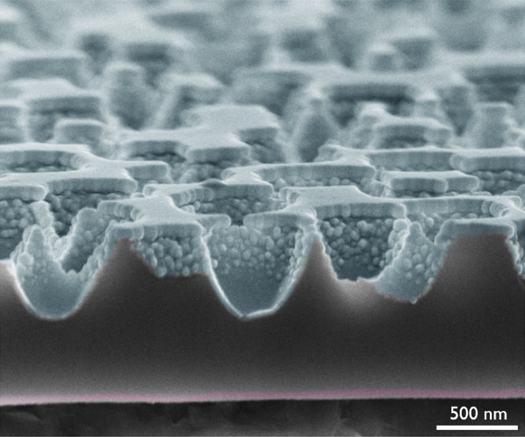
The new method enables the first-time integration of nanocup structures that strongly improve the light absorption of solar cells. (Credit: Depauw et al.)
Standard solar cells feature micron-scale surface textures to enhance the absorption and trapping of light, and shrinking these features to the nanoscale can improve this enhancement even further. The integration of nanophotonic structures has been challenging in the past, however, due to the electrical losses they cause.
Now, thanks to the researchers’ new method, this integration can be achieved without compromising electrical efficiency.
‘We strived to enable the development of a new and disruptive solar cell generation, resulting from the marriage of crystalline-silicon photovoltaics with advanced light-trapping schemes from the field of nanophotonics,’ said Dr Valerie Depauw of Belgian research firm Imec. ‘The core of this project was to bring together researchers from the different fields needed (photovoltaics, photonics, nanostructuring) to interact directly.’
The research team start by separating a micron-thick silicon film from a monocrystalline wafer using a kerfless ‘empty-space-in-silicon technique’ that makes more efficient use of the silicon. An array of narrow pits are etched into the silicon which, upon annealing, form a single planar void beneath the surface. The thin layer remaining above the void can undergo passivation and metallisation before being bonded to a low-cost substrate and removed.
The researchers then imprint a nanotexture by reactive ion etching after shaping the mask from a self-assembled layer of charged polystyrene beads. The result is an amorphously ordered pattern of gently sloping, rounded nanocups, which improve silicon’s light-absorption properties more so than perfectly periodic structures.
Other nanostructures such as nanowires and nanocolumns have been shown to be even more effective absorbers of incident light than the nanocups used by the researchers, however the dramatic increase in surface area they cause in solar cells leads to more recombination losses. High-quality passivation layers and antireflective coatings are also difficult to apply to these other nanostructured surfaces, lowering the overall efficiency of the solar cells featuring them.
The new method and nanopattern used by the team instead represents a compromise between these conflicting needs, and yields an overall conversion efficiency higher than any yet seen for a silicon film of such thinness. The researchers hope this discovery could open the door to new applications for crystalline silicon cells, such as flexibility or semi-transparency, which are not possible with current – much thicker – wafer-based cells.
‘The main applications of our thin c-Si solar cells could be in buildings as windows and skylights, where they will bring more freedom for integration, and possibly lighter and thinner module designs,’ Depauw explained.