Gemma Church finds out about some of the latest developments that are revolutionising the world of digital microscopy
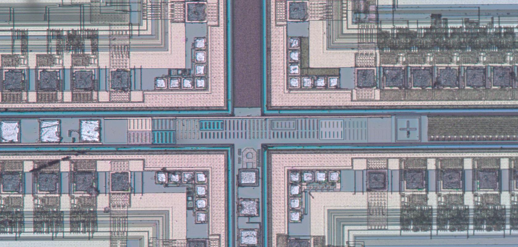
Digital microscopy is an established yet growing field where the equipment found in classic light microscopy is combined with a digital camera and software. Microscopes are employed for numerous applications, such as inspection machines in the semiconductor, PCB, MEMs, gemology and solar cell markets, as for research in well as cytology, pharmacology, biomedical applications, pathology and neuroscience, to name a few from the life sciences.
While there are some instrument variations, each digital microscope contains the same basic components, including an internal tube lens, illumination optics, light source, beam splitter and camera. Another fundamental part is the interchangeable infinity corrected objective lens, which is typically defined by the focal length and the numerical aperture (NA).
Typically, most tube lenses have a focal length of between 160 and 200mm. The ratio between the tube lens focal length and the objective focal length is the overall magnification. Since the spot diameter on the object plane is inversely proportional to the NA, higher NA values yield better resolutions. However, this results in shorter objective focal lengths and an increase in the overall magnification – in other words, a decrease in the object field size.
Decreasing the focal length of the tube lens will reduce the magnification by the same factor, yet maintain the original optical resolution. However, the magnification reduction yields an increase in the signature of the sensor pixel on the object, reducing the cutoff Nyquist frequency. To eliminate this barrier, smaller pixel size sensors are needed. The burgeoning mobile camera market led to the design of sensors with small pixel sizes (0.7 to 2.5 microns) and an ongoing increase in the active areas for these sensors.
This trend has triggered camera vendors to develop industrial cameras with sub-two-micron pixel sizes, opening new opportunities when integrated with low-magnification microscopes.
In its latest whitepaper, industrial microscope supplier Omek Optics examines methods to increase the imaged field of view in standard microscopes. This is a complex undertaking, but one the company has mastered with the recent launch of its miniature Pinky and Omek mic401.80 microscopes.
Maximising success
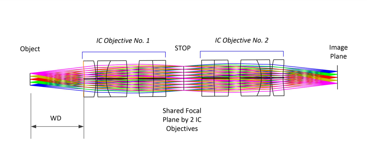
The unit magnification symmetric telecentric relay
Omek Optics has a variety of solutions to deliver Low-MagHigh-NA configurations, while reducing the size and weight of these digital microscopes. The Omek Pinky miniature microscope, for example, is roughly the same size as a computer mouse.
The Pinky aperture STOP is positioned between the two IC Objectives. The magnification and resolution (0.12NA) of the system are fixed. The symmetrical configuration provides telecentricity on both ends, and null transverse aberrations. This overcomes many of the optical design constraints and provides an extremely wide object field.
This design brings many imaging benefits, as Shai Eisenberg, CEO of Omek Optics, explained: ‘The axial symmetry in this design cancels and minimises most of the off-axis aberrations. The optimisation merit function is much reduced, allowing it to acquire larger fields of view.’
Eisenberg added: ‘The numerical aperture of the Pinky microscope is equivalent to that of a standard microscope with 5X overall magnification. However, the field of view area imaged by the Pinky is practically five to 10 times larger. This is a tremendous achievement and the primary focus of our white paper.’
The benefits for the semiconductor industry are prominent both in metrology, alignment and navigation in wafer and PCB inspection systems. The reduced size of the microscope is a key factor in such applications. Eisenberg explained: ‘In this environment, standard digital microscopes consume space, which is costly for the system and add weight on the gantry in question. Many systems include a few microscopes. Systems like the Pinky are small and light, overcoming this issue while providing superior magnification, resolution and extended fields of view.’
Life sciences is another application area where the wide field of view and miniaturisation of the digital microscopes means that measurements can be taken within one space and without moving samples between facilities or different laboratory areas.
Omek Optics recently demonstrated fluorescence imaging with the Pinky microscope. Eisenberg concluded: ‘We’ve only just started to see the potential impact of miniaturised digital microscopes with a high resolution and wide field of view. It’s an exciting space to be working in now.’
To overcome the wide field challenge, a totally different and opposite approach has been adapted by some vendors, according to Eisenberg. ‘They simply scale up the entire system, including the microscope, objective and camera sensor to enlarge the imaged field of view.’
While this ‘brute force’ strategy has been used for more than a decade, there are drawbacks to this approach. Eisenberg explained: ‘These digital microscopes are large and heavy. They also require large CMOS camera systems and dedicated custom objectives, making them expensive and cumbersome instruments.’
Find out about the various options in digital microscopy to enlarge the object size yet maintain the original resolution by downloading the latest white paper. It will discuss and compare various methods, emphasising the advantage of Omek Optics solutions with consideration to the formats and pixel size of the imaging camera and the optical layout of the microscope.
