
Advancing synthetic diamond production is enabling new photonics technologies, however a number of challenges still remain in serving quantum applications, writes Dr Ian Friel, Business Development Manager at Element Six
Driven by key technology trends and market needs, the last decade has witnessed significant progress in the development of a number of commercial and emerging photonics technologies which harness the exceptional physical properties of diamond. This progress has been made possible by innovations in the synthesis of optical quality diamond by chemical vapour deposition (CVD), in diamond colour centre engineering, and in the techniques used to manufacture diamond optical components and photonics structures.
Photonics applications based on diamond’s outstanding intrinsic properties
Intrinsic, or highly pure, diamond is optically transparent from the ultraviolet to terahertz frequencies and beyond. It has the highest room temperature thermal conductivity of any bulk material (greater than five times that of copper), and possesses a low thermo-optic coefficient. These properties make diamond optical components ideal for high-power industrial laser applications, including machining, welding and additive manufacturing, across many different parts of the electromagnetic spectrum. Additionally, diamond is the hardest substance known and is exceptionally stiff and strong, so is highly suited to defence and security applications requiring rugged optical and infra-red components, capable of performing in highly challenging environments.
Optical quality CVD diamond comes in both single-crystal and polycrystalline forms. Polycrystalline diamond has the advantage of being available in large areas of up to 135mm in diameter. An example of the use of optical polycrystalline diamond is as a window for the high power, 10.6µm CO2 lasers used in extreme ultraviolet (EUV) lithography systems for state-of-the-art semiconductor device manufacturing nodes. This technology, motivated by the drive to maintain the pace of Moore’s law, is critically dependent on diamond windows synthesised and processed to rigorous optical quality standards, as no other optical material can operate under the extreme laser conditions required.
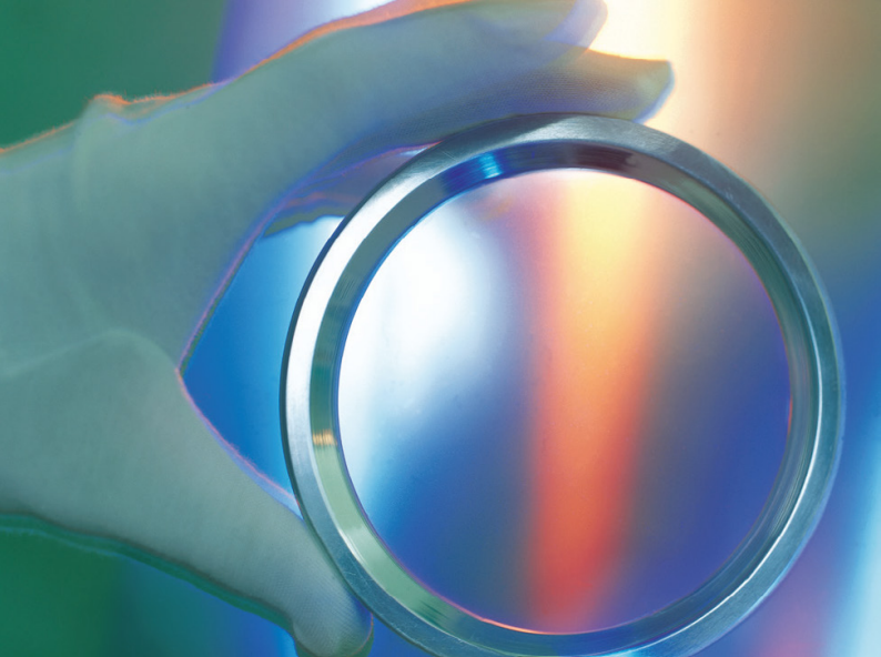
For industrial lasers, large area polycrystalline CVD diamond optics are more robust and reliable than the ZnSe optics they typically replace (Image: Element Six)
At wavelengths shorter than around 1.5µm, scatter losses in polycrystalline CVD diamond mean that most applications in this range are addressed using single crystal diamond. Due to the size limitations of currently available diamond substrates, single crystal diamond components are typically around 5 to 10mm in length and, although several producers are developing large area single crystal diamond on non-diamond substrates, such material cannot be used for all optical applications due to its relatively high internal strain.
Despite the size limitations, several single crystal CVD diamond-enabled photonics technologies have been developed, such as diamond Raman lasers, based on Element Six’s unique low optical absorption, low birefringence crystals. These nonlinear lasers use the phenomenon of stimulated Raman scattering to convert a pump beam into a Stokes-shifted output beam, thus extending the range of available laser sources for new applications from the UV to the IR, including materials welding, 3D printing, directed energy, lidar, remote sensing and laser guide stars. Diamond has one of the highest Raman gain coefficients, which, combined with its high thermal conductivity, make it an ideal gain medium for demonstrating power scaling and brightness enhancement, including in the “eye-safe” spectral region from 1.4 to 1.8µm, in which the available choice of laser sources has previously been limited.
Expanding diamond’s application space through colour centre engineering
In addition to its superb intrinsic optical properties, diamond plays host to several hundred different optically-active defects, or colour centres. Several of these are of significant interest for technological applications that utilise the quantum states of light and the electron spin properties of the colour centre, including quantum communications, quantum computing, and a range of sensing applications. In particular, the nitrogen-vacancy (NV) colour centre has been the subject of intense research due to the ability to easily manipulate its quantum state via the application of light and RF-fields, for single defects as well as ensembles, at room temperature.
Depending on the end application, the NV centre can be created via two approaches. One is through the controlled incorporation of nitrogen during the CVD growth process, which distributes nitrogen atoms throughout the material at a desired concentration. The other, where precise spatial control of individual colour centres is required, using nitrogen implantation. Lattice vacancies are then generated by irradiation with high energy electrons, and the crystal is annealed at high temperature to mobilise the vacancies into combining with the nitrogen atoms in the crystal, thus forming NV centres. Similar approaches can be taken to form other colour centres of interest, such as the silicon vacancy (SiV) or germanium vacancy (GeV) centres.
For quantum information processing, arrays of colour centres are required which allow both control over their quantum properties, and a means to efficiently couple individual centres together, via photonic cavities. Due to diamond’s chemical inertness and the lack of wide market availability of wafer-scale single crystal diamond, developing the nanofabrication techniques needed for such structures has required considerable effort and investment, but much progress in this area has been achieved in recent years. This includes the fabrication of sophisticated nanostructures in the form of waveguides, pillars, cavities and disks using a variety of lithographic techniques and employing both plasma and reactive ion beam etching.
Challenges in enabling diamond quantum photonics
Significant progress has been made in the production of diamond with high intrinsic optical quality, and high-quality colour centres, enabling a number of new and existing advanced photonics technologies. In the field of diamond quantum photonics, several challenges remain before scalable chips, for applications such as quantum information processing, can be realised. These include: improvements in the engineering of colour centres and robustness of qubits; wafer-scale fabrication; and hybrid integration with other photonic materials and components. Despite these challenges, research in these fields is intense and dynamic, and substantial progress can be anticipated in the coming years.
Further reading
- R. Mildren and J. Rabeau, Optical Engineering of Diamond. John Wiley & Sons, 2013.
- “Element Six Diamond Handbook.” 2021. [Online]. Available: https://e6-prd-cdn-01.azureedge.net/mediacontainer/medialibraries/eleme…
- S. Sarang and M. Richardson, “Power Scaling of CW Crystalline OPOs and Raman Lasers,” Photonics, vol. 8, no. 12, pp. 565-, 2021, doi: 10.3390/photonics8120565.
- M. Kianinia and I. Aharonovich, “Diamond photonics is scaling up,” Nat. Photonics, vol. 14, no. 10, Art. no. 10, Oct. 2020, doi: 10.1038/s41566-020-0695-9.
- P. K. Shandilya et al., “Diamond Integrated Quantum Nanophotonics: Spins, Photons and Phonons,” J. Light. Technol., vol. 40, no. 23, pp. 7538–7571, 2022, doi: 10.1109/JLT.2022.3210466.