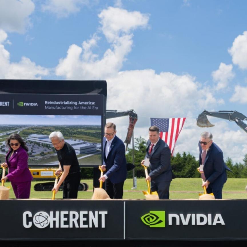
Nokia expands capacity for photonic chip test and packaging in US
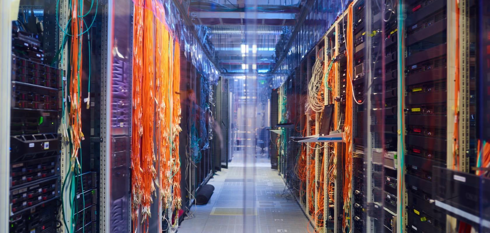
Nokia is expanding its test and packaging site in the US, strengthening America’s semiconductor supply chain for AI data centres (Image: Nokia)
The expansion in Pennsylvania is part of a multi-year $4bn investment plan in preparation for AI network connectivity
Register for FREE to keep reading
Join 15,000+ photonics professionals staying ahead with:
- Exclusive insights, funding alerts & market trends
- Curated newsletters and digital editions
- Access to The Photonics100 list of R&D champions
- Exclusive panels & roundtables for professional development
- Technical White Papers & product updates to guide smarter decisions
Sign up now
Already a member? Log in here
Your data is protected under our privacy policy.