Siemens reports over 10 times faster EUV lithography simulation with new technique
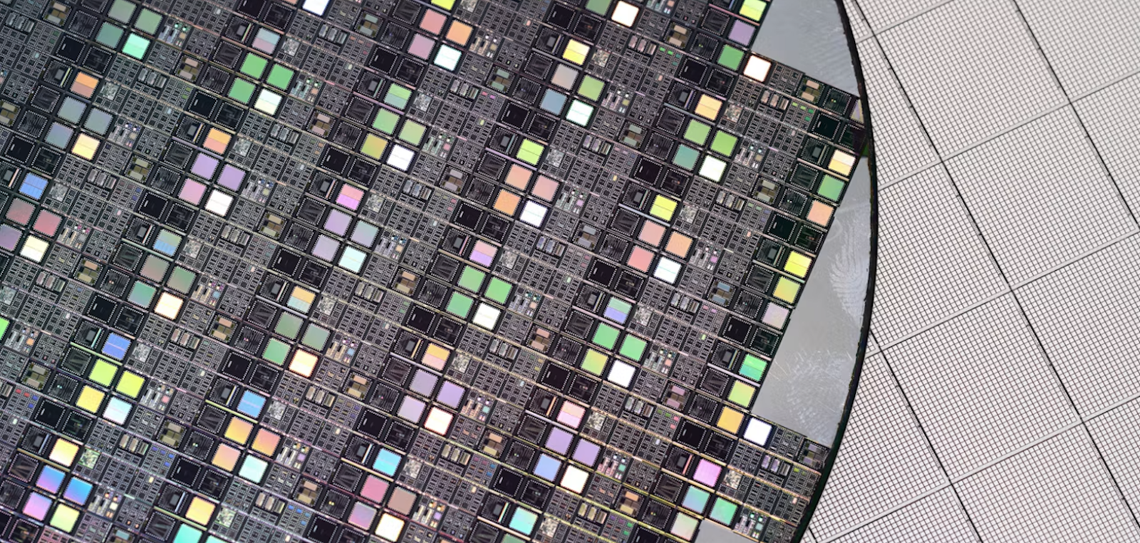
Siemens says its new lithography simulation technique addresses the critical runtime and complexity challenges of leading-edge patterning for AI compute and memory devices (Image: Siemens)
The company says its collaboration with Nvidia will help speed up computational lithography methods and support complex patterning for advanced AI chips

Register for FREE to keep reading
Join 15,000+ photonics professionals staying ahead with:
- Exclusive insights, funding alerts & market trends
- Curated newsletters and digital editions
- Access to The Photonics100 list of R&D champions
- Exclusive panels & roundtables for professional development
- Technical White Papers & product updates to guide smarter decisions
Sign up now
Already a member? Log in here
Your data is protected under our privacy policy.