The sub-micron semiconductor challenge: how is it being met?

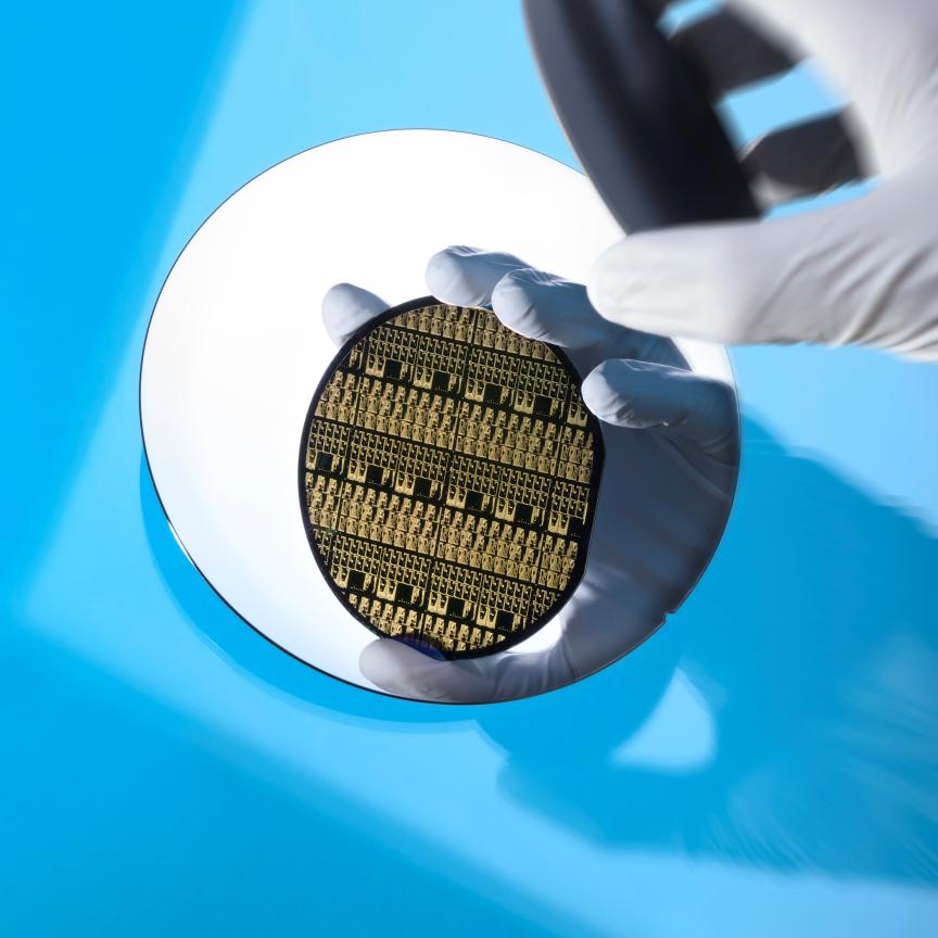
Ensuring optimal measurements and quality of wafers and chips early on is vital for long-term semiconductor operations (Image: Wikimedia Commons)
Interferometry, microscopy and spectroscopy are helping meet the need for accuracy in semiconductor inspection and measurements at sub-micron levels.
The continued innovation of computing technologies relies on the manufacturing and deployment of semiconductors, which are gradually reducing in size. With this comes the growing need to inspect and measure integrated circuit (IC) components including chips and wafers at sub-micron and nanoscale levels – and mechanical probes and traditional optical microscopes are proving insufficient.
Register for FREE to keep reading
Join 15,000+ photonics professionals staying ahead with:
- Exclusive insights, funding alerts & market trends
- Curated newsletters and digital editions
- Access to The Photonics100 list of R&D champions
- Exclusive panels & roundtables for professional development
- Technical White Papers & product updates to guide smarter decisions
Sign up now
Already a member? Log in here
Your data is protected under our privacy policy.