A team of researchers has discovered how to precisely control and monitor the growth of tin-based thin film coatings when applying them to silicon nanometre-structured surfaces.
Published in Small, the work could open up new applications in the fields of biophotonics, energy generation and mobility.
Tin-containing thin films can be used to bestow specific optical and electrical properties to surfaces, making them desirable for a wide variety of parts and components in electronics, sensors and photovoltaics.
For example, they can be used in surface-enhanced Raman scattering (SERS) spectroscopy as UV-SERS-active surfaces. In addition, tin-coated anodes can ensure high electronic conductivity in high-performance lithium-ion batteries, for electromobility and thermal energy storage.
Researchers from the Leibniz Institute of Photonic Technology (Leibniz IPHT), together with scientists from the UK, Germany and Russia, have been observing and investigating the development process of such nanoscale tin layers.
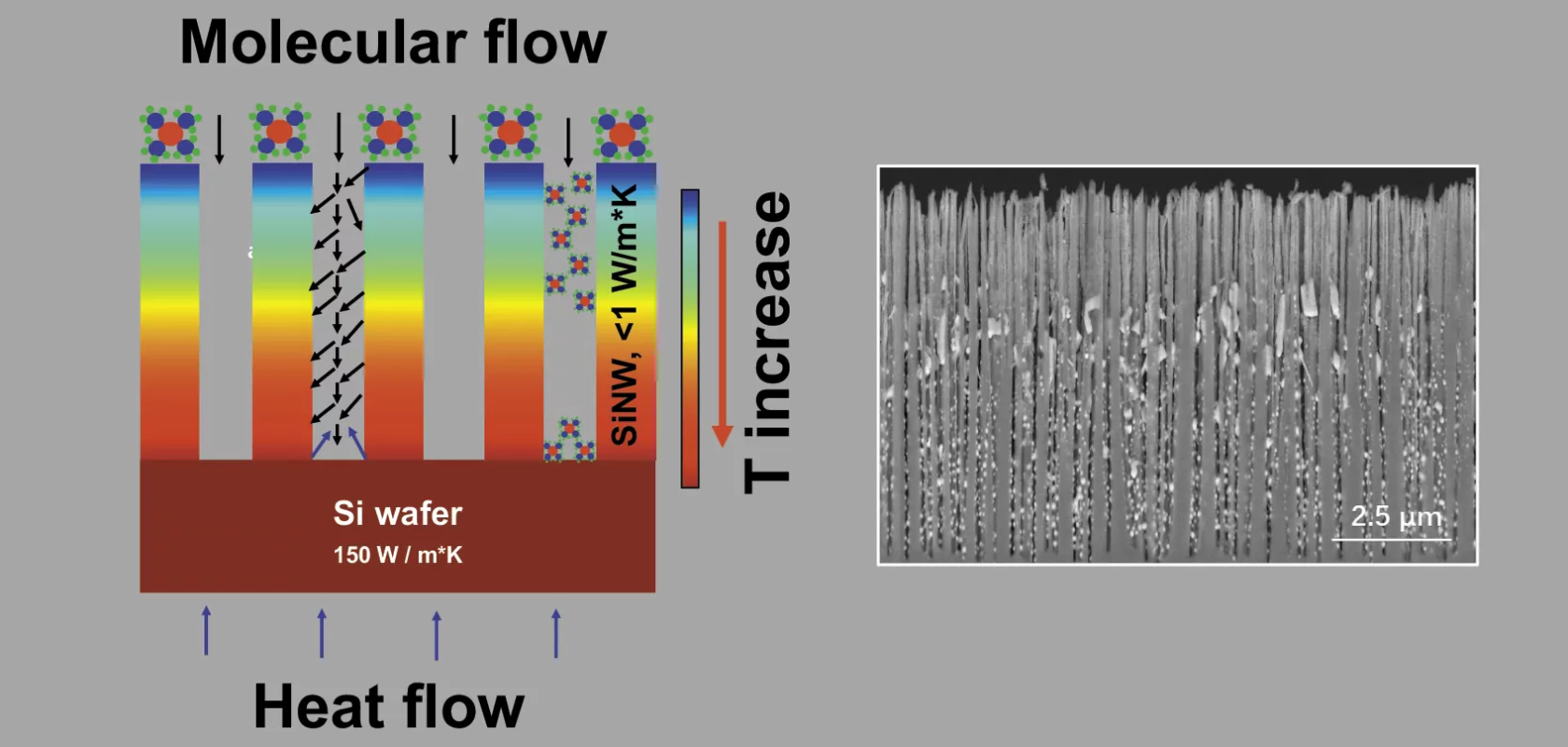
In experimental studies, they were able to demonstrate, for the first time, a specific distribution effect of tin along silicon-based nanowires less than 100nm in diameter. Tin-containing layers with different degrees of oxidation were formed along the entire length of the semiconductor nanowires by means of metal-organic chemical vapour deposition at a deposition temperature of 600°C.
The researchers investigated the growth dynamics of the observed tin-based layers using microscopic and spectroscopic methods. In contrast to planar and unstructured silicon surfaces, on which deposition takes place homogeneously, the surfaces of the semiconductor nanowires were covered with tin-containing crystals of different sizes and shapes over the entire length.
The results presented in Small show the formation of different tin oxide phases along the nanostructured silicon surfaces, which could be identified with tin dioxide (SnO2) in the upper part, tin monoxide (SnO) in the middle part and with metallic tin (Sn) in the lower part. According to the researchers, the amount and distribution of the formed metallic Sn and its SnO and SnO2 oxides can be explained and effectively controlled via the length, diameter, porosity, and spacing of the silicon-based semiconductor nanostructures.
In addition to these geometrical parameters, the team was able to reveal the formation of hydrocarbon-containing by-products as reducing agents for tin oxide reduction as another factor influencing the distribution of the formed tin layers along the semiconductor nanostructures.
The thermal conductivity of the silicon structures and thus the temperature distribution along the nanowires during the high-temperature vapour deposition can also have an influence on the formation of different tin oxide phases.
“By understanding how tin coatings grow and which factors influence this growth process, we create the conditions for specifically controlling coating processes,” explained Dr Vladimir Sivakov, head of the Silicon Nanostructures Group at Leibniz IPHT. “This allows surfaces to be refined very precisely and to be equipped with desired functional properties at previously defined positions.”
The work was done within the project “Development and atomic and electronic structure characterization of functional Sn/SnOx surfaces for SERS-based analysis of misfolded proteins”, which was funded by the German Research Foundation (Deutsche Forschungsgemeinschaft, DFG).