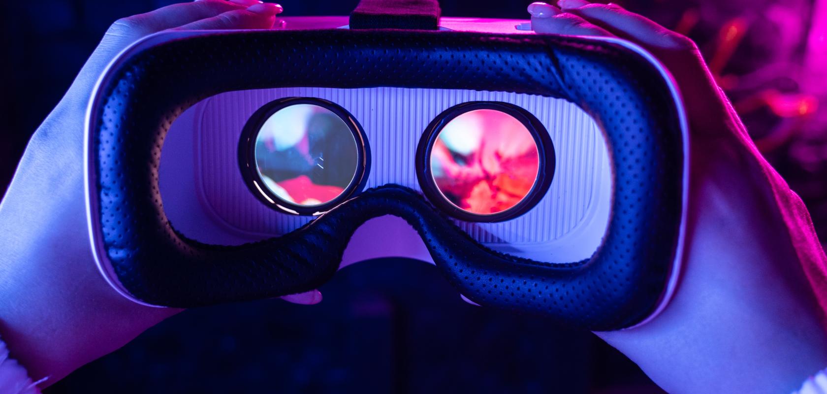
The use of complex or freeform optics has the potential to deliver high performance with compact design, including lightweight and achromatic solutions in reflective applications. Interest in developing these innovative complex optics is being largely driven by the predicted growth for augmented, virtual and mixed reality (AR/VR/MR) headsets and related devices as more people and organisations enter the ‘Metaverse.’
Such optical innovations will enable wearable Metaverse devices that require fewer components, leading to more compact optical systems with increased imaging quality that are smaller, lighter and more efficient. These developments will also, find application in other 3D sensing and machine vision systems and applications.
A recent report from industry market research company, IDTechEx, sees a 24 per cent compound market growth for such ‘meta’ optics over the next decade.
Applying uniform optical coatings to complex or freeform optics is not a trivial task, however, a new spatial atomic layer deposition (ALD) system, jointly developed by Finnish technology company, Beneq with Laser Zentrum Hannover (LZH) in Germany, has demonstrated uniform coating of complex-shaped optics. The innovative system achieves higher deposition rates than previously possible through ALD.
LZH and Beneq developed the device together, explained Gerd-Albert Hoffmann, head of the Optics Integration Group at LZH, combining LZH’s knowledge of optical coating and Beneq’s extensive expertise on ALD processes. Beneq launched the world’s first industrial production using ALD in 1984.
ALD technology produces very thin, high-quality coatings and, so far, has been used primarily to produce thin functional layers in the semiconductor industry. The new Spatial ALD system now makes applications in other highly demanding industries economically viable.
‘ALD as a coating process is well-known,’ Hoffmann said. ‘But the significant difference between our new ALD and standard batch ALD devices is that it is in the category of Spatial ALD systems. Normally in the ALD process, consecutive steps lead to layer growth based on self-limiting chemical reactions between gaseous precursors and the substrate surface in one chamber, with processed gases exchanged one after another. This makes it a time-resolved, or series production of the layers.
‘In the new machine all the states necessary for the ALD process are available at the same time,’ he continued. ‘The different process steps are separated spatially, and the substrate components pass through the different process steps by rotating around the process chamber.’
The new system has four individual process chambers separated by pressure differentials and nitrogen. Within each chamber, one ALD half-process step can be completed. The substrates then rotate into the next chamber for the next process step. This makes the process economical while, in parallel, allowing high throughput in optical coating applications.
Researchers in LZH’s Optics Integration Group have used the system to produce layer systems of uniform thickness much faster than before, including on strongly curved and structured optics. Other coating methods, such as ion beam sputtering or electron beam evaporation, are limited in this respect.
Faster deposition
The new device allows a much higher deposition rate, explained Hoffmann: ‘We are looking at one micron per hour compared to one micron per day, which is currently achievable. And optical coatings need a lot of layers with alternating materials, which takes a considerable time with normal ALD processes. But with the Spatial ALD process, you can achieve much higher efficiency, which means quicker production or the ability to deliver more complex layered systems in a sensible timescale.’
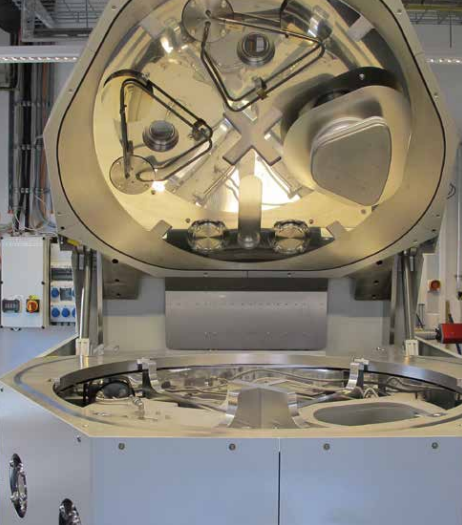
The plasma-based Spatial ALD system operates with rotation and can precisely coat even complex-shaped optics. Credit: LZH
The key to the new spatial process is the ability to monitor via optical monitoring the growth of the coating layers in situ.
‘The optical monitoring is achieved using a device developed by LZH – the Broadband Monitor (BBM),’ says Hoffmann. ‘The performance of the Spatial ALD is based on the capability of the BBM. With it, we can observe the growth of layers and react if the rate of deposition is deviating from the original design. This allows optimisation of the layers.’
The feature could also allow process automation, but currently, the best option is to have an experienced coating technician on hand to oversee the process.
Spatial ALD should be especially appropriate for special optics. The Spatial ALD system can achieve layer coating growth rates similar to IBS and other technologies, but can tackle more complex forms. ‘The Spatial ALD system can tackle coating of not only planar shapes, but also free-form substrates, or forms with structured surfaces with very small feature sizes or very high aspect ratios, such as grooves in diffraction gratings,’ said Hoffmann.
Other coating technologies have issues with depositing uniform coatings that conform to these free-form shapes, he explained: ‘They rely on a mechanism that applies the coating in one direction, or is focused on a specific direction. But ALD can produce a very good conformal coating, even if the surface is not directly pointed to the plasma. The reactant gas is all around the part you want to coat. It is everywhere, so it can penetrate the grooves or other surface features to react and initiate the layer deposition. The shading effect is very small or even non-existent.’
With its high deposition rates and ability to produce ultra-thin coating systems for complex optical surfaces, Spatial ALD could be of interest in the fields of automotive lighting or AR/VR, where three-dimensional shaped lighting elements are essential. Also, it can operate at low temperatures (below 100 degrees centigrade), because it is plasma-based. This makes it particularly suitable for coating temperature-sensitive polymer optics.
Coatings for structured and freeform optics for use in AR and VR applications are exactly the markets foreseen for the new ALD system. Hoffmann’s team is also working on 3D-printed optical components using different materials – glass or polymers – that may also find use in these applications.
One big area that Hoffmann foresees for Spatial ALD is in integrated photonics. ‘This is an area where companies are continually looking to make things smaller, better integrated and cheaper,’ he said. ‘Cheaper photonic integrated circuits and photonic integration, in general, is a very big current topic.
‘Spatial ALD could make a lot of sense here,’ he concludes. ‘You could imagine using Spatial ALD to apply coatings directly onto components on the assembly carrier itself.’