Higher power lasers and ultrafast pulses are putting greater demands on the thin film coatings protecting the lenses in these systems. Complexity of thin films is increasing, with the number of layers reaching into the hundreds and coating runs lasting days. All of this requires precise deposition machines, and, in recent years, a number of companies have incorporated in-situ broadband optical monitoring into the coaters to improve precision and avoid costly errors.
There has also been a resurgence in thermal evaporation techniques, according to Chris Cook, principal engineer at Edmund Optics. Most precision optics are still coated with evaporation techniques – they are the most versatile and best understood – whereas more energetic techniques like sputtering are generally considered to give higher quality coatings. However, this generalisation might not necessarily hold true in all cases.
‘Some of the best laser damage threshold results being reported have been achieved with conventional (unassisted) thermal evaporation techniques,’ stated Cook, adding that they are better in some cases than more energetic processes such as ion beam-assisted deposition (IAD), an improved form of thermal evaporation, or even sputtering.
Although conventional thermal evaporation tends to result in some porosity in the coatings, that doesn’t seem to be a limitation for achieving high laser damage thresholds (LDT) in many cases, Cook said.
Evaporation can work with the widest variety of materials and generally has the lowest cost and greatest versatility in terms of the size and shape of optics that can be coated. Sputtering, on the other hand, uses sputter targets which are expensive and, also, the machines are limited to a certain number of these targets per run. ‘A pot of evaporation material might cost a couple of hundred pounds, whereas you might invest two or three thousand pounds for a sputter target,’ Allan Jaunzens, marketing manager at Evatec, commented.
The fact that evaporation techniques are producing films with high laser damage thresholds is ‘somewhat counter-intuitive to many in the field’, Cook commented.
‘Currently there’s a lot of effort going into understanding why certain energetic deposition techniques produce films with such varying LDT results,’ he said. ‘The mechanisms that drive LDT in optical coatings are not completely understood, but many researchers are focusing on defects within the coating layers as a main driver.’
In addition, even deeper explorations are ongoing into the fundamental mechanisms of defects, Cook added. This research not only looks at defects inside the coating layers, but also defects at the surface that arise from pre-deposition conditions including the way optics are polished and cleaned, and exposure to ion-beams prior to deposition.
Dr Yubong Hahn, chief scientist and founder of Rocky Mountain Instrument (RMI), makes the point that the quality of the optics, how they are manufactured, has a significant impact on the quality of the coating. ‘The quality of the substrate’s surface is the starting point of any kind of coating development. Even cleaning and preparing the substrates for coating is critical,’ he said.
RMI has recently begun a programme to develop more consistent measurement tools, including systems to measure the surface quality of the substrate before coating. The company is also developing laser damage threshold measurement equipment to test the finished optic, (currently LDT systems are only designed for YAG and CO2 laser wavelengths, but RMI is aiming to expand the capabilities into the ultraviolet).
Optical monitoring
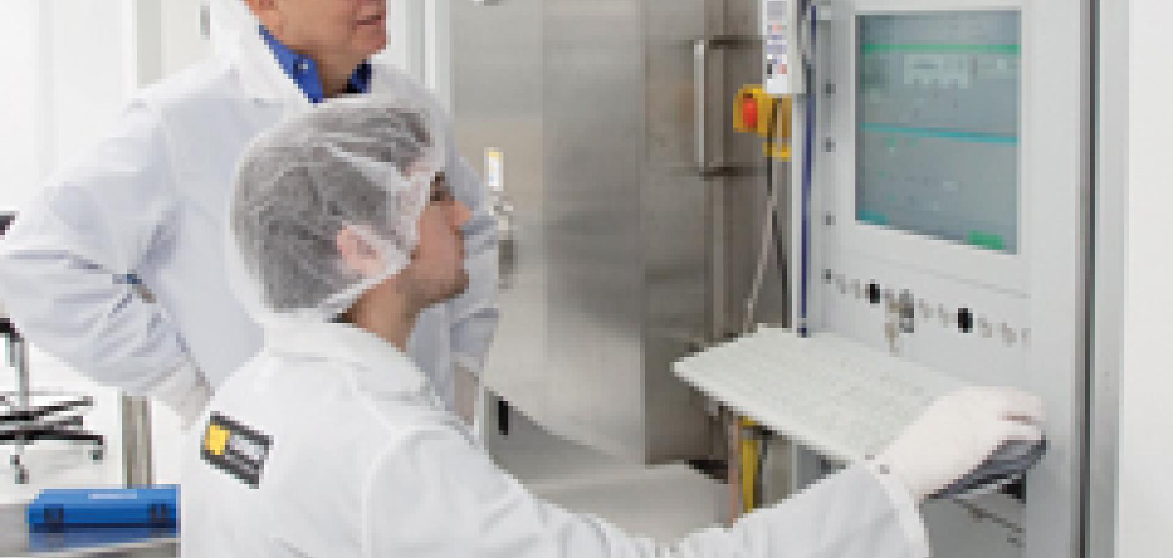
With some coating runs lasting days, the need for advanced process control is now greater than ever. In-situ broadband optical monitoring is now part of many companies’ coating machines, whereby optical performance can be measured after each layer is deposited during the coating run, rather than at the end.
‘If there’s any deviation from the ideal optical performance during deposition, the machine can adjust the remainder of the process downstream to obtain the planned optical performance,’ explained Jaunzens. ‘This type of closed-loop control is relatively new and enables you to tune the process during coating for tightening of tolerances or improvement of yields.’
Last year, Evatec launched its updated in-situ broadband optical monitoring capability for its coating machines, called in-situ re-optimisation.
One traditional optical monitoring technique is quartz crystal monitoring, whereby the resonance frequency of a quartz crystal is measured to get a readout of the thickness of the coating directly. An alternative is narrowband optical monitoring that looks at the change of reflection or transmission of a witness substrate in the coating chamber at one wavelength only. Quartz crystal monitors are typically about ±5 per cent accurate, while narrowband techniques are in the 1-2 per cent range of accuracy, Cook noted.
Broadband optical monitoring covers the entire spectrum, in-situ, during the coating process. ‘Instead of matching to just one point as in narrowband monitoring, you can potentially match to a thousand points, and therefore proportionally increase the level of accuracy,’ Cook said. ‘Applying this technique in direct mode, i.e. looking at the light through the optic within the sample area of the dome or planetary, the accuracy can be even greater.’
Broadband optical monitoring uses a spectrophotometer that looks at the reflection from or transmission through the substrate as the coating material is deposited. It terminates the layer when the optical performance reaches the desired level. ‘It’s a direct measurement, rather than an indirect one,’ noted Jaunzens. This means the process can be tweaked layer by layer in a closed-loop process. ‘The system will tune the coating process after each layer, so that even in the case of a mismatch for any single layer, the recipe for the remaining layers can be adjusted to ensure the optical performance of the end filter or optic is still within specification,’ he said.
Cook commented: ‘Since the coating machine itself can now monitor the entire spectrum in real time and identify when it is making errors, the errors can be potentially corrected by adjusting the design of the subsequent layers to compensate. This is the first time to my knowledge that this capability is being offered commercially by coating machine manufacturers. The advancements in technology relative to in-situ metrology alone are going to have a big impact on the ability to produce coatings at higher rates, higher yields, and higher throughputs – it’s a big deal.’
One of the limitations in optical coating deposition is test runs. ‘Test runs can consume a great deal of machine capacity, and they affect the whole enterprise of coating fabrication in terms of its ability to turn things around at a reasonable and reliable rate,’ commented Cook. By employing in-situ broadband optical monitoring, ‘the run itself becomes its own test run, and thus has a unique capability of minimising the number of test runs and increasing productivity,’ he added.
Coating software
Other advances in coating technology involve the software. Professor Steffen Reichel at the advanced optics division of Schott said that developments in the coating simulation software follow improvements in the coating machines. ‘As soon as you know your coating machine is capable of producing highly precise layers, then you can use the coating software to design more sophisticated layer stacks,’ he said.
The progress in coating software can also generate challenges for coating vendors. ‘As software for designing and producing coatings is improving, there can be a challenge in finding a suitable substrate. For example, super-polished substrates are required to achieve the highest performance, but it is very difficult to produce this finish on a curved substrate,’ explained Gemma Micklewright at Laser Components.
Laser Components employs physical vapour deposition, ion assisted deposition (IAD), and ion beam sputtering (IBS) at its optical coating facility, and Micklewright commented that most of the company’s chambers now use in-situ metrology. ‘IBS and IAD coatings are where the benefits allow for extraordinary and complex coatings,’ she said, adding that without in-situ metrology such designs would not be possible – ‘without an online monitoring system a small error could result in 15 or more hours of time wasted’.
Ion beam sputtering now has the same deposition rate as magnetron sputtering, noted Reichel, which equates to a relatively high throughput and makes the technique more suitable for industry. The IBS layers can also now be deposited with greater homogeneity over the coating area.
A further advance in IBS is that modern sputtering machines are capable of using three coating materials, rather than just two, according to Reichel. ‘In former times you used a high index layer and a low index layer. Now you can use three different layer types with different refractive indexes without opening the machine,’ he said.
This gives additional freedom for the layer design. For example, silicon dioxide could be used as the low refractive index material and titanium oxide as the high index layer, as well as another material with a refractive index in between, such as aluminium oxide. ‘Three different coatings give the thin film design software more freedom to find a solution to the optical problem. Three coating materials also improve the interference filters,’ Reichel said.
Reichel sees a move towards sputtering technology. ‘The layer produced with sputtering is better, both in terms of thickness accuracy and homogeneity. Ion beam sputtering produces a very smooth very low-defect coating,’ he said.
‘We are seeing increasing requests for IBS,’ added Steven Hahn, CEO of Rocky Mountain Instrument. ‘IBS is most effective in the visible and NIR, from around 300nm to 2µm, because the techniques and chemicals for IBS processing have been developed more in that region.’
IBS is ideal when there is a very tight specification regarding bandpass cut offs and damage thresholds that require dense coatings with many layers. Evaporation techniques still retain the lion’s share of optical coating tasks, but sputtering has its place and its use is only likely to increase.
High-performance coatings are needed to separate very close wavelengths in applications like fluorescence imaging, noted Gemma Micklewright at Laser Components. Further examples requiring advanced coating techniques include broad dielectric coatings for systems using multiple light sources, and the coatings for dichroic filters used in applications like microscopy, she said.
Mike Scobey, CEO at optical filter manufacturer Alluxa, commented: ‘Optical coatings continue to advance in precision and performance for a wide variety of applications including life sciences, Raman spectroscopy, lidar, semiconductor, and scientific markets. They are offering spectral profiles that are squarer, with higher transmission and deeper blocking, and tighter wavelength control than ever before. Combining these attributes means, for example, fluorescence excitation or emission filters can be made to discriminate spectral features separated by only a few nanometres and reject six optical densities, and still provide transmission levels of 90 per cent.’
Alluxa can provide flat-top multi-cavity temperature stable filters of 0.5nm bandwidth across the UV to the NIR. The company offers ultra-narrow filters up to diameters of 100mm, which, noted Scobey, are useful for lidar systems, laser cleanup, or anywhere a user is detecting narrow laser light.
Thin film coating company, Iridian Spectral Technologies, is working on a project to provide optics for imaging lightning, among other environmental phenomenon. ‘Here, the optics are on the order of 6-8 inches, and the coating has to be applied uniformly to look at one particular spectral line,’ said Jason Palidwar, account manager at Iridian. This means the coating has to be very well controlled for performance across the entire part, he added.
‘In a satellite application, you might want to observe multiple phenomena with one detector to save cost and weight,’ Palidwar continued. This might involve taking a single detector and turning it into a multispectral analyser by creating filters that have spatially varying spectral performance. ‘We did some work for the Canadian Space Agency on a filter the size of a Canadian penny with 10 different bands on it in the mid- and long-wave infrared, and high precision in each of the individual bands. Those bands are combined to create a multispectral optic,’ he said.
Iridian is also coating complex telecom filters, which Palidwar said, are in excess of a thousand layers and the coating runs taking several days. ‘This has also driven a need for in-situ optical monitoring and automation of the decision making processes,’ he said.
Along with satellites and astronomy, other markets that are pushing the coating technology include high laser-induced damage threshold optics, lithography, and the biomedical market, noted Professor Steffen Reichel at the advanced optics division of Schott.