Micromachining is one of the fastest-growing industrial applications for lasers. Initially adopted as a more agile and rapid alternative to conventional technologies, laser micromachining is increasingly central to production of the next-generation of today’s fastest-growing new technologies, such as solar cells and biotech lab on a chip’ devices. Laser micromachining is displacing conventional technologies in these areas not only because it is simpler, cheaper and faster, but also because it is proving able to create the complex, detailed microstructures that conventional micromachining techniques are unable to provide.
Laser micromachining is typically performed by one of two methods. Excimer lasers use a mask in a similar way to laser lithography. This produces superior edge quality and throughput, and can handle complex patterns cleanly. DPSS and ultrafast lasers use a direct write method, which provides faster setup and easy integration to CAM systems.
Revving up the firing rates
Efficient laser micromachining faces a number of technical challenges. At low laser energies – such as infrared – molecular vibration and rotation can produce excessive heating of materials. At high energies, molecular dissociation and ionisation can affect the worked material. Laser micromachining typically employs pulsed systems at long or ultrafast speeds coupled with bandwidths that minimise local damage to materials, such as ultraviolet and infrared.
A key issue with production pulsed lasers for micromachining is the rate of duty cycle. Conventionally, many high-speed pulsed lasers have had very low duty cycle rates, reducing their utility in high throughput micromachining applications. Increasing the repetition rate of picosecond and femtosecond lasers is bringing these technologies increasingly into the high volume commodity manufacturing field. Ultrafast lasers produce clear benefits in terms of reduced thermal damage and improved accuracy. But nanosecond lasers have higher repetition rates and their beams are stable and capable of longer pulse working without the significant plasma damage that ultrafast lasers can generate. They also tend to be simpler and cheaper to maintain than their femtosecond cousins, making nanosecond lasers the standard industry workhorses for laser micromachining.
Some vendors have recently switched their attention to picosecond lasers, with Lumera Laser of Germany and Oxford Laser of the UK producing picosecond micromachining systems.
According to Oxford Laser, picosecond lasers combine most of the advantages of both nanosecond and femtosecond lasers, while avoiding the disadvantages. They provide good micro material processing, with minimal thermal damage and high precision, while also offering very high repetition rates and avoiding plasma damage.
More power from solar
With soaring oil prices and mounting concerns over global warming caused by fossil fuels, it makes both economic and environmental sense to look at clean energy alternatives such as solar power. This has led to tremendous growth in the solar energy industry. Photovoltaics, the segment of the industry focusing on electricity generation from sunlight, is growing at around 40 per cent per year. This rapid growth is thanks to improvements in solar cells made possible by laser micromachining.
The bugbear of alternative energy technologies is efficiency. Fossil fuel technologies contribute to global warming, and fossil fuels such as oil and gas are subject to rapid price inflation. But fossil fuel technologies are well-established and a single plant is capable of generating high energy output. Technologies such as nuclear and new generation coal are cleaner, cheaper alternatives to today's conventional power generation technologies that are still capable of producing very high energy outputs. To compete, solar energy generation must approach the output efficiency and return on investment of today's conventional generation plants as well as next generation alternatives such as nuclear and clean coal.
Efficiency in early solar cells was affected by a number of factors. Circuitry to collect energy generated by each cell ran across the surface, obscuring sunlight and reducing cell efficiency by 10 per cent. Another factor was edge short-circuiting: an excess of semiconductor material at the edge of each wafer could lead to the cell short-circuiting and power generation being lost.
Laser micromachining has helped remove both these problems, improving the output efficiency of solar cells. Laser-etched solar cells have cut the amount of surface area obscured by circuitry by half, while laser edge insulation has helped eliminate short-circuiting.
As production volumes step up and price points become more sensitive, so lasers are being replaced in some processes by cheaper, higher volume etching technologies. In edge insulation – once a key area for laser micromachining in photovoltaics – chemical processes are taking over as a cheaper, high volume production process.
However, far from losing ground in solar cell manufacturing, as some laser shops fear, laser micromachining is likely to expand. The over-riding need to increase cell efficiency is leading to new technologies that will require more laser micromachining. In line with other semiconductor device manufacturers, solar cell producers are also aiming to shrink unit sizes still further. This increases efficiency, boosts output and cuts costs. To meet demand and maximise return on expensive solar cell fab facilities, vendors are aiming at significantly higher output volumes. To meet all these objectives, solar cell manufacturers are likely increasingly to replace mechanical drilling and sawing with laser micromachining.
The conventional design of the solar cell – with circuitry etched onto the surface – could soon be replaced with more radical designs to improve panel yield. Germany's Institut für Solarenergieforschung has developed a cell with circuitry behind the cell rather than on the surface. The energy yield improvement is considerable. However, to produce such cells at production speeds, costs and quality requires pulsed infrared micromachining.
Laser manufacturer Trumpf believes that highspeed short pulsed lasers are likely to replace conventional materials processing in manufacturing next generation thin layered solar cells. They will prove, the company believes, faster, more accurate and cheaper.
The challenge is in developing lasers that can pattern the highest performance solar cells made from copper, indium and selenium. This calls for laser beam widths of 20μm, a positioning accuracy of one micrometer, and picosecond pulse durations. It must also be capable of high speeds. Trumpf argues that picosecond lasers are increasingly capable of achieving such high throughput performances: its own can fire 200,000 times per second.
Biotech’s next generation
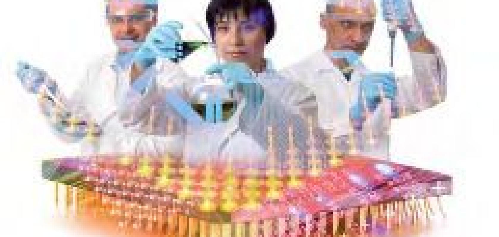
Laser micromachining is poised to play an increasing role in the fast expanding field of biotechnology. A key component of biotechnology is the biochip. A silicon composite, biochips typically comprise two types. The first is the microarray, a plate for microtitration, featuring anything between six and 6,144 sample wells for reaction testing. This is the standard workhorse of analytical biochemistry and clinical diagnosis, giving it a wide and fast expanding range of applications in healthcare and pharmaceutical drugs development. The second is the more complex microfluidic biochip, designed to move fluids or particles over networks of channels into a whole range of successive or separate tests and measurements. By emulating the complex processes and workflow of conventional testing facilities, microfluidic biochips are often labelled ‘labs on a chip’.
The challenge in manufacturing each type of biochip is addressing the necessarily complex interplay of materials within the device to achieve rapid, agile and cost-effective production. Conventional production techniques are neither particularly rapid nor agile. Nor are they especially cost-efficient, except at very high volumes. They are also complex, capital intensive and a challenge to manage. By contrast, laser micromachining offers an approach that is simpler, less capital intensive, rapid and agile, and more cost-efficient at lower volumes.

Jewel – Rofin produces a micromachining laser specifically for the jewellery industry.
Biochips use a broad range of materials that can pose real problems of biocompatibility. These include glasses, polymers such as polyimide, polycarbonate, PMMA, epoxies, thin metal films, bulk metals and elastomers. For conventional production technologies such as photolithography, this diversity of materials can be a major problem.
Developments in established devices such as microtitration arrays are increasing the challenge for conventional production technologies. Conventional microarrays are passive devices with external optical test and measurement. Increasingly, microarray plates are incorporating active technologies for test and measurement that are multiplying the complexity and biocompatibility issues in the production process.
The UK Laser Manufacturing Centre, together with the Institute of Bioelectronic and Molecular Microsystems at the University of Wales, has carried out a range of trials to prototype and manufacture biochips. They employed an Exitech S8000 Excimer micromachining workstation, as well as a Spectra Physics Hurricane Ti:Sapphire femtosecond laser integrated into an Exitech M2000F workstation.
Their conclusion was that laser micromachining provides a complete, integrated solution for manufacturing complex active microarray biochips that is simpler, faster and cheaper than conventional non-laser micromachining, and well suited to both prototyping and rapid volume manufacturing, with quality equivalent to more complex and costly production techniques.
The team also examined the suitability of laser micromachining for manufacturing more complex microfluidic ‘lab on a chip’ devices. They found the use of grey-scaling or half-toning dithered algorithms allowed highly contoured smooth manifold structures to be created with laser micromachining that matched or surpassed sophisticated conventional techniques, at far more cost-effective rates.
Laser micromachining is better able to handle complex structures involving multiple materials, and does not suffer biocompatibility issues. The UK Laser Micromachining Centre and University of Wales team believes that laser micromachining offers not only the cheapest and fastest technology for producing ‘lab on a chip’ biotech devices, but the most advanced and biocompatible as well.
Jewellery that flies
Most laser micromachining involves large systems deployed in large-scale industrial settings. One exception is in jewellery, where small firms are adopting small and inexpensive micromachining systems such as the EasyJewel from German vendor Rofin-Baasel.
Originally designed for marking precious metals, working jewellers have extended EasyJewel's application to micro-letter engraving onto gemstones. The result is inscriptions on precious stones with lettering less than a millimetre in size. Exact facsimiles of handwriting can be reproduced at the micro-scale with great accuracy. Engraving a gem can be performed in only a few minutes. Inexpensive laser micromachining has allowed the development of new forms of personalised jewellery not possible with conventional micromachining.
Laser micromachining has also transformed the setting of precious stones. Using EasyJewel, jewellers have developed new techniques for setting gems in metal that minimise the setting mount and open the way for startling new jewellery designs. Filigree welding of great delicacy is made possible. The new laser technique avoids the heavy pressure usually applied to gemstones with conventional setting techniques, which can crack the corners of finely cut gems, not only endangering their value, but limiting the jeweller’s freedom of design cutting with the gem itself. The result is new, freer, almost transparent designs, liberating gemstone and metal from the heavy settings of the past.
Making possible some of tomorrow’s most exciting new technologies – including the next generation of biotech and clean energy devices – laser micromachining faces new opportunities. While some of its first applications transition to higher volume conventional techniques, laser micromachining’s unequalled flexibility, materials handling and accuracy are creating new openings at the forefront of micro-scale technology development.
As solar is a ‘renewable’ energy, there is a strong pressure to utilise ‘green’ equipment in the manufacture of solar cells. According to Finlay Colville of Coherent UK, lasers represent a true ‘green’ manufacturing compared to alternatives. An example is laser edge isolation, where lasers scribe an isolation groove, typically 10-20μm deep, to eliminate shunt pathways between the front and rear surfaces where established alternatives include plasma and wet-chemical etching technologies. ‘Of the various tools used for edge isolation,’ says Colville, ‘only DPSS lasers provide a near-ideal “green” tool, thanks to their high electrical efficiency (using single-phase electrical input) and closed-loop water-cooling. In fact, this is now one of the single biggest applications for both our nanosecond Avia and Prisma lasers and our picosecond Talisker lasers.’
But the use of DPSS lasers for edge isolation is not only enabling greener edge isolation, it also increases yields and improves device efficiency. Specifically, current generation systems are now relying more heavily on DPSS lasers operating at either visible (532nm wavelength) or ultraviolet (355nm), because of the significantly higher absorption of c-Si at these shorter wavelengths. Silicon absorption is some four to five orders of magnitude stronger at 355nm, compared to the infrared (1064nm), allowing highly localised front surface scribing when using Q-Switched UV DPSS lasers. In addition to shorter penetration depths, UV wavelengths allow narrower grooves to be scribed in a colder ablative process with minimised peripheral thermal damage, such as microcracks, which are potentially yield-killing. This enables the grooves to be located closer to the cell edges, while the overall yield advantage of non-contact processing will become more important as the solar industry moves to thinner, more fragile wafers.
Colville points to thin-film type solar cells for an example where the tailored performance of the latest generation of DPSS lasers is enabling higher throughput. These lasers are routinely used to generate discrete cell isolation and interconnection strips by scribing up to a few hundred thin lines on each of the three layers deposited during the panel production stage. The limiting speed of optical scanning technology means that multiple laser beams must be used in parallel, so power requirements are modest.