Among the remarkable optical feats that smartphones achieve, delivering millions of high-quality aspheric lenses per day is one of the more impressive.
Typically for aspheric lenses, there is a tradeoff between volume and quality – but not in smartphones, says Merten Kuna, field application engineer at Mahr. The powerful photography they enable needs high-accuracy asphere manufacturing – but the sheer volume means that it’s impossible to test every lens. Kuna explained that the polymer lenses are made by moulding, using a diamond-turned metal mould as a master.
Manufacturers ‘put a lot of effort’ into making those master moulds high quality, to avoid introducing errors into the lenses, Kuna stressed. It falls to companies like Mahr to enable this impressive process through metrology. Freeform optics is another complex technology that plays an important role in highly specialised optical applications that are set to impact consumer electronics. In this area, metrology companies are moving closer to meeting precision requirements ‘step by step’, Kuna said.
That’s necessary because, in recent years, challenges in aspheric and freeform optics have grown such that metrology systems have struggled to reach the precision needed. Modern optical polishing techniques can remove material at the nanometre level, but measurement techniques are not able to measure with the same precision. ‘Measurement traceability for aspherical surfaces is about 50nm,’ said Hichem Nouira, principal research scientist at the French National Laboratory of Metrology and Testing, LNE. As such, reaching nanometre-level precision would take a lot of work, Nouira said, so LNE has worked with industry to help achieve this.
Freeforms are used for off-axis optical systems, ‘especially those that need to be very compact,’ explained Jessica DeGroote Nelson, director of technology and strategy at prototype optic manufacturer Optimax. In such systems, the optical axis is not aligned with the system’s mechanical centre.
‘Two examples of applications that use freeforms are wearable or head-up displays and space-borne telescopes. Wearable or head-up displays are possible mid- to high-volume optics, whereas space-borne telescopes are typically very low volume.’ They demand high accuracy measurements of surface irregularities and, as they are often asymmetrical, basic positional and location information to confirm orientation.
One main category used for measuring freeform and aspherical optics is single point probe metrology, which gradually builds up maps of lenses from physically mapping their shape. Coordinate measuring machines with a scanning head can provide accuracy of approximately 1µm. Such techniques can be contact or non-contact and can measure most asphere and freeform geometries, DeGroote Nelson highlighted. While they have historically been slow and can scratch surfaces, she stressed that single-point probe metrology ‘continues to advance to minimise errors, to produce higher precision measurements’.
Interferometric testing can pass a laser beam through or reflect it off a freeform or aspheric optic, studying interference with a reference beam to find unexpected path deviations. It often gives users higher resolution information, which results in the ability to test surfaces in higher precision. For example, the Panasonic UA3P ultra-high accuracy profilometer combines an atomic-force measurement probe combined with displacement interferometry to track the position of the probe in x and y directions. This metrology tool can produce data accurate to approximately 50nm – but only for surface angles below 30°. ‘Interferometric testing has limitations on the geometries or surface slopes that can be measured,’ DeGroote Nelson explained.
Pumping up the volume
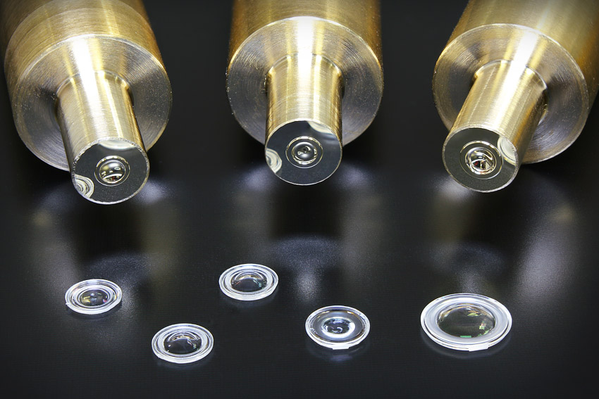
Smartphones have adopted aspherical lenses because they require fewer elements that are needed for optical correction, explained Stefan Krey, managing director at Trioptics. Objective lenses can therefore become smaller and lighter. Mobile phone objective lenses exclusively use highly complex aspherical lens surfaces to produce the desired image quality in the smallest volume possible. Such aspheres are plastic moulded lenses, found in high volume smartphone cameras and very expensive professional camera equipment.
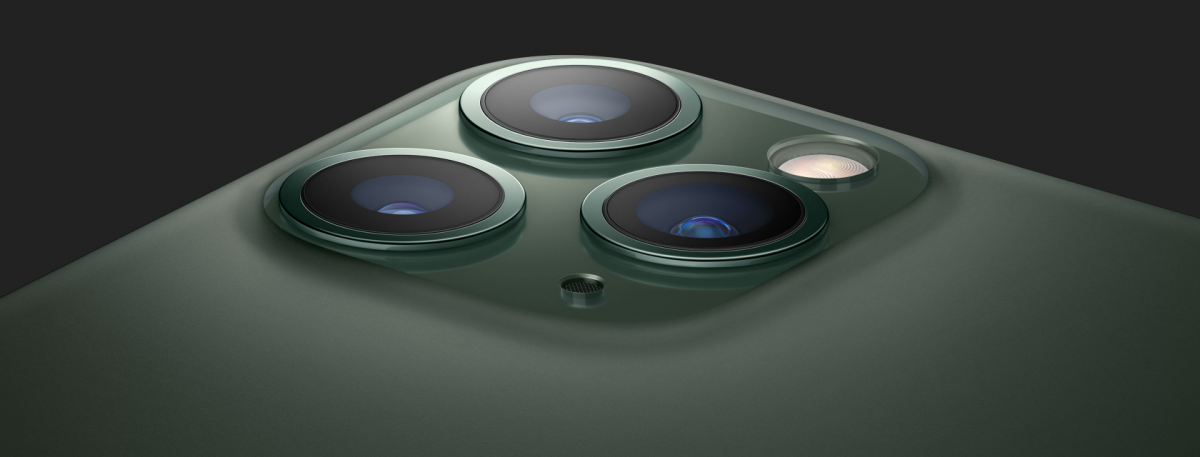
Many smartphones contain aspherical lenses, such as the iPhone 11 pro shown here. Credit: Apple
As aspheres become even higher quality in low-volume specialised applications, they are fabricated in glass, Krey explained. ‘Manufacturing of aspheres in traditional glass grinding and polishing processes is very expensive due to several iterative manufacturing and measuring processes,’ he said. However, glass moulding is now reducing this effort. It might become ‘the standard in mid- to high-volume glass asphere production,’ Krey said.
In consumer electronics, traditionally a contact probe device is used for measuring asphere moulds, noted Dan Musinski, vice president of strategic business development, Zygo. But these approaches have inherent low resolution and users find it difficult to measure the full surface in a reasonable timeframe, often taking more than an hour per measurement. These challenges result in manufacturers having to make assumptions about the symmetry of a moulded part. ‘This can be risky given the many sources of potential deformation and the tighter manufacturing tolerances,’ said Musinski. ‘As mobile device companies introduce new generation higher resolution cameras, they need metrology that can verify the required specifications, such as surface form, defects and mid-spatial frequency characteristics, along with inhomogeneities in the material.’
Zygo’s Compass optical profiler exploits coherence scanning interferometry (CSI) to enable such capabilities. It uses a six-axis stage that keeps the lens surface normal to the objective, ensuring reliable data is captured all across the lens. Proprietary stitching algorithms then bring together data from the different parts to create a detailed 3D map of the entire lens surface. Compass is typically used to characterise the aspheric and freeform surfaces of small diamond-turned moulds and plastic lenses used in consumer electronics applications. Zygo’s Verifire Asphere interferometer, a semi-automated workstation, utilises a patented acquisition technique for the fast measurement of larger circularly symmetric aspheres.
However, metrology is often an afterthought, Musinski added. He feels that firms often define desired performance and create an optical design that can enable this. They adopt the latest manufacturing techniques and only then bring the finished product to the quality lab for measurement. Zygo has created a calculator for the Verifire Asphere that predicts the measurability of an asphere design before the part is manufactured. Code V optical design software from Mountain View can also optimise designs based on whether or not it can be measured with the Verifire Asphere, Musinski noted.
Going to extremes
Some applications are also especially challenging, Musinski added. Semiconductor and consumer electronics continue to ‘push the limits of traditional metrology techniques’, he said. ‘The semiconductor industry represents the primary user base for extremely high quality large aperture aspheres, up to approximately 320mm diameter,’ Musinski explained. ‘These are made from high-quality glasses and used in projection lens assemblies for lithography and various metrology instruments used for process control. There are very few companies that have the capability to manufacture this type of asphere, and they typically use a combination of commercially available and proprietary techniques to verify their performance.’
Mahr’s Kuna highlights the use of freeform mirrors used in today’s most advanced extreme ultraviolet lithography (EUV) techniques. ‘As microchip structures get smaller and smaller, you need EUV. If you want to shape radiation like this, you can only use reflective components.’ This is the application with the lowest production numbers but the highest accuracy requirement, Kuna stressed. Optics used in satellites, such as space-borne telescopes, are also produced in ‘very limited numbers’, Kuna added. He noted that such optics require very high surface accuracy, thermal stability, low weight and shock resistance, ‘especially when you consider the rough conditions they are used in’.
Illumination asphere optics for general and automotive lighting are the opposite extreme, with high volume and low accuracy requirements, as they are tolerant to beam deviations. ‘Maybe 50 per cent of the lenses made are just thrown away because it would take too much effort to correct them compared to just producing a new batch,’ he said. In such mass production contexts it is common to adapt Fizeau interferometers used to measure spherical lenses to measure aspheres and freeforms using computer generated holograms (CGH). The approach exploits a faceplate etched lithographically to put in diffractive elements to change the shape of the optical wavefront.
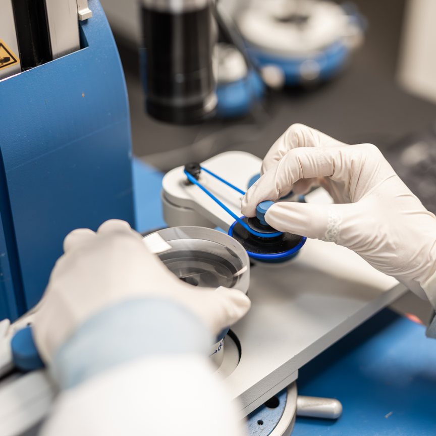
Mahr supplies interferometric tools that are ready to be used with CGH, and point probe tools. But Kuna highlights that it has now combined interferometric and tactile point probe functions in its MarForm MFU200 Aspheric tool. ‘The tactile probe is used to contact mechanical references known as fiducial marks on the optical component and align it on the machine,’ he said. ‘Then, we use the optical probe to measure the optical surface and evaluate it according to the coordinate system, defined by the mechanical fiducials.’
Trioptics’ Krey said that design of aspheres and freeforms has got simpler thanks to today’s design software. Now defining opto-mechanical tolerances and measuring the optics’ form are the main issues. ‘You are not really sure what you will get out of your process and you have
to take into account several iterative cycles,’ he said. ‘Tight process control is the key.’
Krey added there is not yet a ‘gold standard’ for asphere metrology and sees different approaches as competing. ‘It seems the point sensor methods are the most versatile’ for complex aspheric and freeform designs ‘but are limited by their mechanical precision and slow speed’.
Attention to detail
Trioptics produces its Opticentric line of tools to focus on one key opto-mechanical parameter, the intrinsic centring of the asphere. ‘Most aspheres are designed rotationally symmetrical, because most objective lenses work rotationally symmetrically around the optical axis,’ Krey explained. ‘In standard spherical optics you can correct a tilted optical axis of an individual lens element by proper mounting. This is not possible with aspheres. The asymmetry is an intrinsic property of the lens, and is either in or out of tolerance.’
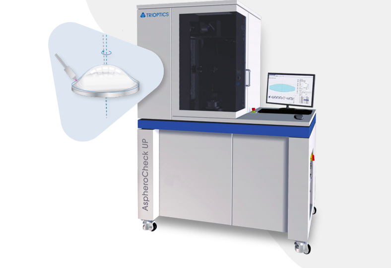
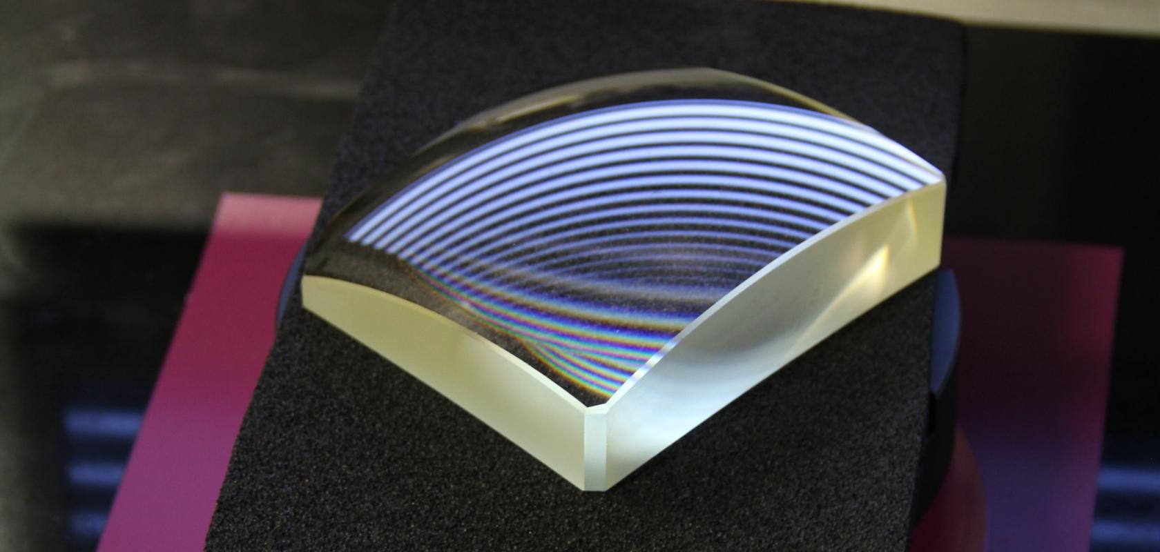
The OptiCentric AspheroCheck (pictured above) measures the deviation of the rotational symmetry of aspheres, Krey explained, in conjunction with non-contact probes. ‘It uses an autocollimator and a second optical profiler for the measurement,’ Krey said. ‘Sometimes additional mechanical contact probes are used to locate mechanical reference surfaces, flanges and mounts.’ Such challenges mean that Trioptics has been involved in several projects dealing with asphere-form metrology.
For example, Trioptics was an unfunded partner in the European FreeForm project, led by LNE’s Nouira, that was completed last year. Mahr was also ‘very active’ in the project, which improved the metrology chain and traceability for aspherical and freeform optics, enabling reliable data analysis with measurement uncertainty below 30nm. ‘Improvement of measurement uncertainty at National Metrology Institutes (NMIs) improves the capability of industry to measure parts,’ Nouira said. ‘Any developer of measurement instruments can claim to have the best measurement instrument’, he added, but without traceability to an NMI that can’t be confirmed.
Reliable surface metrology is critical for the ‘deterministic sub-aperture polishing’ step for high-value aspheres and freeforms, DeGroote Nelson highlighted. ‘The initial surface error map is used to create the manufacturing sub-aperture dwell map,’ she explained. ‘After polishing, measurement is used again to verify the convergence of the polishing run. If there are errors in the initial measurement, then they will be polished into the part.’
Optimax’s in-house research has been focusing on another fast, versatile non-contact technique that can help with this, known as deflectometry. In this approach, a camera images fringe patterns that have reflected off a surface under test. The system can deduce a map of the surface slopes from the deviation of the projected fringes, and from that determine the surface shape. Optimax works on using deflectometry measurements on mid-spatial frequency measurements, error features that can be induced by the subaperture polishing techniques used in the manufacturing process, to reduce the potential small-angle scatter, DeGroote Nelson said.
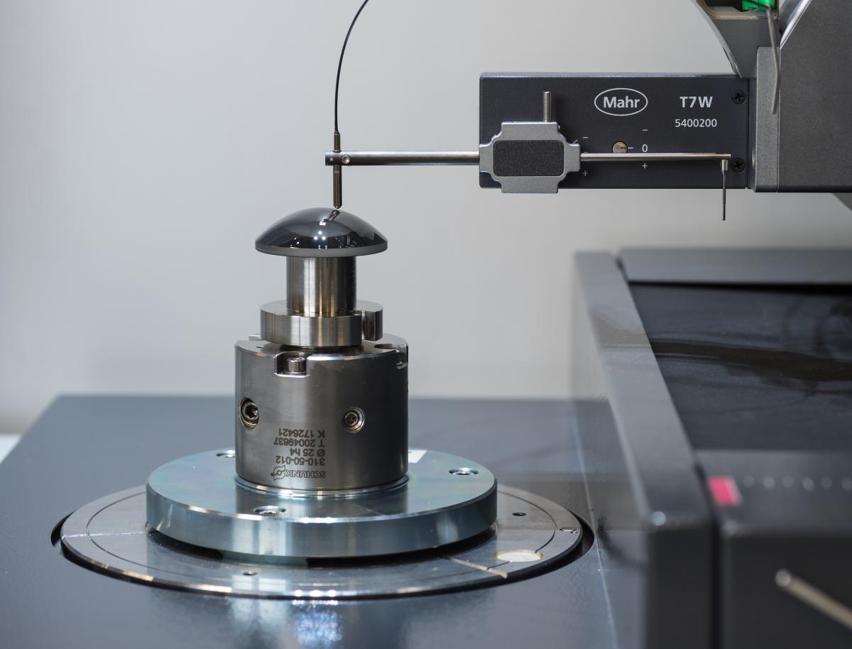
Mahr’s MFU200 tool uses an optical-tactile working principle
Using such techniques, Optimax, and the industry more broadly, are taking the next steps in improving metrology.
Exploiting the latest tools and techniques, these capabilities are set to push freeform and aspheric optics onto their next challenges. With the consequences potentially as significant as helping ensure the continuing increase in computing power the semiconductor industry seeks to provide, it is vital that they succeed.