The optical measuring equipment market is buoyant and still growing. The latest Optical Metrology Market by Product report data from P&S Intelligence predicts a global reach of $2,945.3 million by 2023.
Leading the global markets, says P&S, will be China, thanks mainly to a rising demand for optical metrology equipment for surface inspection and measurement of automotive parts, supported by increasing production of vehicles, as well as government initiatives for electric vehicles. However, a key driver for this growth is, arguably, the semiconductor industry, which needs precise measuring equipment to ensure any issues are highlighted early enough in the manufacturing process to prevent months of work becoming invalid. The report also highlights a rise in inspecting for cracks and defects in oil and gas pipes, as well as metrology for healthcare and manufacturing markets.
In healthcare 3D scanners are used for a number of applications, such as prosthetic and orthotic device design, automated measurement of medical components, implant research, and plastic surgery. They also provide full-field geometric data to inspect medical devices made of plastics, and for further processing in computer-aided design and manufacturing (CAD/CAM) processes in dentistry. Growth in the global manufacturing industry, meanwhile, prompted more demand for first article inspections, acceptance testing, and benchmark testing, and the tools used to manufacture precision parts must also be accurate and free of defects. Laser scanners, in particular, are required for measuring dimensions.
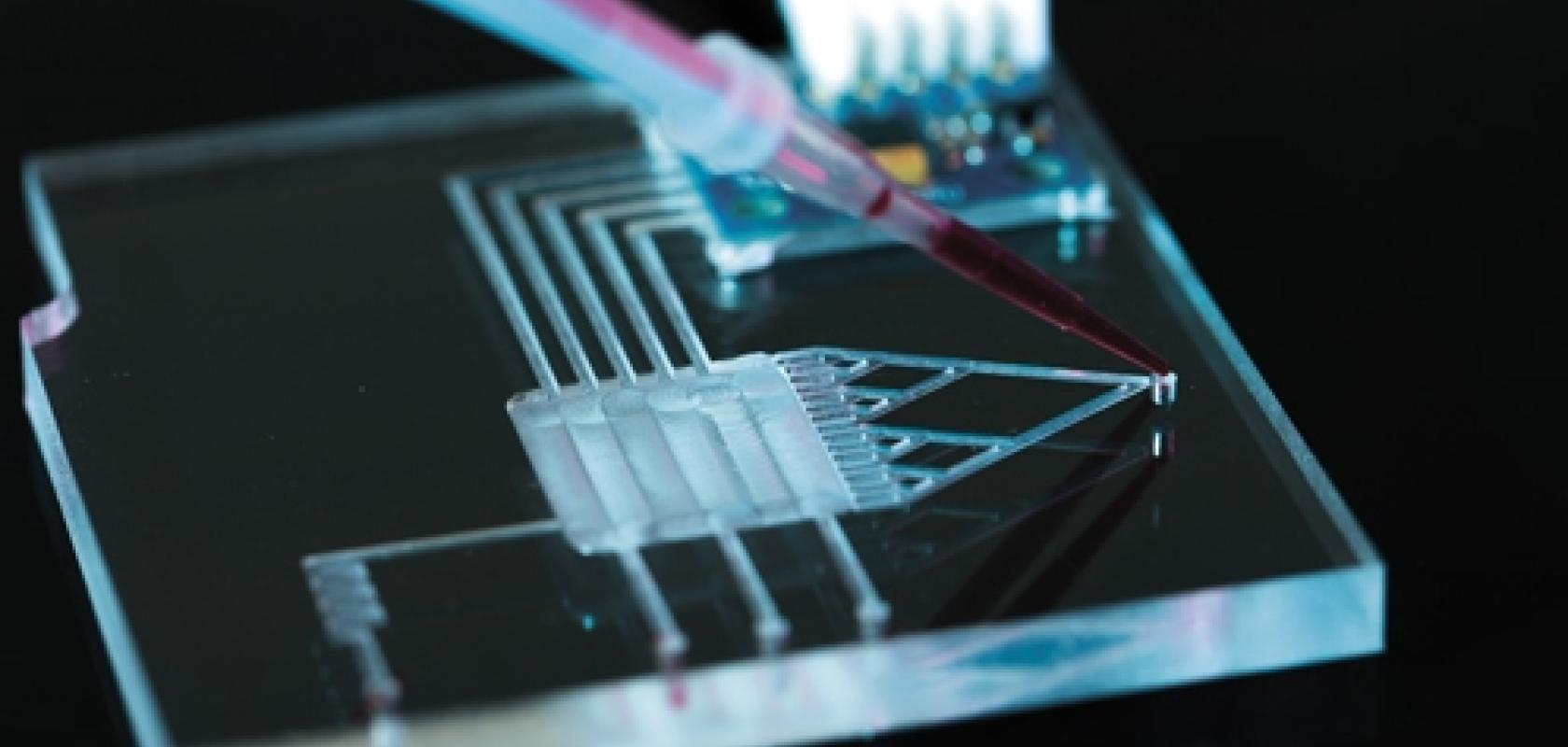
One application for which optical metrology has proved itself to be particularly effective is in microfluidics, which has experienced enormous developments in the past few years. Lab-on-a-chip, organ-on-a-chip, point of care devices, cell capture, chemical and biological analysis are some of the examples for direct applications dealing with the flow of liquids inside micrometre-sized channels. Advances, such as the systems behind 3D surface topography, have enabled the success in areas such as this, as Sensofar Metrology found out during its partnership with Photonics4Life, a research group in the Optics Area of the Applied Physics Department of the Universidade de Santiago de Compostela in Spain.
Complexity as required
Scientists at the university had been fabricating different microfluidic devices using laser processing. These devices have different geometries which can be as complex as needed, but one of the basic structures etched into the device is the microchannel. Ricard Mollon, marketing specialist at Sensofar Metrology, explained: ‘Several materials have been reported for the fabrication of the microchannel, and the suitability of one or another depends on the fabrication technique. Some of these materials are polymers, silicon or glass. Examples of manufacturing techniques are soft-lithography, photolithography or thermofusing techniques. But when using soda lime glass as material – which was chosen for the research due to its robustness, chemical resistance, transparency and low cost – direct laser writing presents itself as one of the most suitable techniques.’
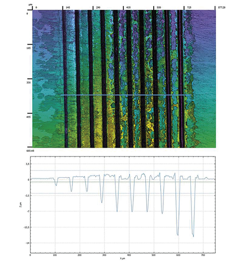
Confocal image of several microchannels with different laser scans, from one (left) to ten (right). Credit: Sensofar Metrology
This is thanks to the laser’s high accuracy and versatility, generating complex geometries at speed. What’s more, because of its non-contact nature, there is no contamination and so does not require clean room facilities. ‘When working in micron dimensions for this application,’ continued Mollon, ‘it is crucial to have a very good image of the topography, to ensure its quality, as well as all the information about the channel dimensions. In this report, the structures manufactured by direct laser writing are fully characterised by means of confocal microscopy.’
Sensofar Metrology’s devices are based on confocal, interferometry and focus variation techniques. Confocal profilers measure the surface height of smooth to very rough surfaces, with spatial sampling as low as 0.10µm. White light vertical scanning interferometers (VSI) measure the surface height of smooth to moderately rough surfaces, providing nanometre vertical resolution, regardless of the numerical aperture, to make use of all available magnifications to profile shape features. Focus variation was developed for measuring the shape of large rough surfaces and the company uses this method to complement confocal measurements at low magnification. This combination of methods has been used in applications from standard research and development setups and quality inspection laboratories to complete non-contact metrology solutions for in-line production processes.
Aspect ratio
For the microfluidic work, researchers fabricated the microchannels over soda lime glass by direct laser writing. The laser employed was a Rofin Nd:YVO4 system, with 20ns pulse duration and 1,064nm central wavelength. The setup used a galvanometer system that allows the fabrication of complex structures with no need of sample movement. The laser beam was focused over the substrate surface by using a lens of 100mm focal length that ensures a working area of 80 x 80mm2.
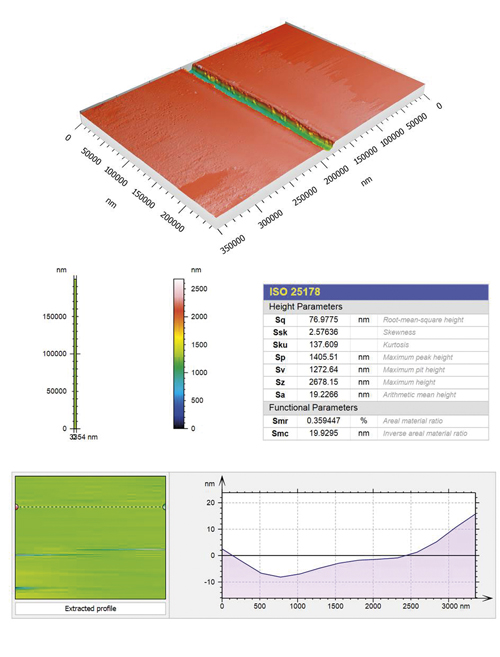
3D topography of one microchannel fabricated with a laser, and the roughness parameters of the bottom of the channel according to ISO 25178. Credit: Sensofar Metrology
In order to obtain a proper aspect ratio of the structures, several laser scans were applied to the sample, and so a study of the evolution of the topography was performed. Microchannels with scans from one to ten times were manufactured.
Using Sensofar’s S Neox 3D optical profiler, a confocal image of the structured area was captured using a 20X magnification objective. The surface profile was generated and the evolution of the depth of microchannels with the laser scans was depicted.
‘Roughness value of the microchannel walls are a critical value to know,’ said Mollon, ‘since it should be low enough for microfluidic applications. Thanks to the optical profiler and SensoMAP analysis software, it was possible to obtain roughness values from small areas. The topography of the bottom of a microchannel with eight laser scans, obtained with a 50X magnification objective, was selected for the study.
‘Thanks to the versatility and accuracy of laser direct writing, several microfluidic devices can be manufactured. Thanks to our optical profiler, it was possible to easily characterise the topography of the microchannels fabricated with laser technologies. The evolution of the profile of the structures with the laser scans was analysed by using the confocal technique with a 20X magnification objective.’
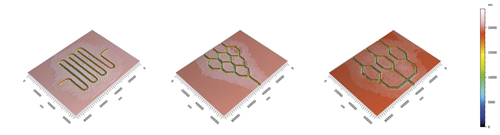
3D confocal topographies detail some examples of microfluidic devices performed with laser over soda lime glass. Credit: Sensofar Metrology
Channel calculations
In combination with Sensofar’s analysis software, the roughness parameters of the manufactured channels were calculated. In this case, a 50X magnification objective was employed when acquiring the confocal topography. In conclusion, said Mollon, ‘by using the S Neox 3D optical profiler, each structure can be perfectly characterised in dimensions and roughness.’
For 4D Technology, some of the biggest recent developments in optical metrology equipment come in a Fizeau interferometer – an interferometric arrangement that places two reflecting surfaces facing each other. The rear-surface reflected light from the transparent first reflector is combined with front-surface reflected light from the second reflector to form interference fringes.
While the technology has been around for some time, it has evolved, from fringe counting, to fringe tracing software, to phase shifting and beyond, as Steve Martinek, director of sales and marketing at 4D Technology, explained: ‘There were beam expanders and families of products with interchangeable accessories. Radius of curvature measurements have come a long way. Then there were instantaneous measurements, and – with our dynamic interferometry breakthrough – there are now single frame, single-image phase-shifted measurements. Since the early days of laser interferometry, optical manufacturers have depended on Fizeau interferometers as the workhorse of the polishing shop.’
Error minimisation
One of the reasons behind this is that the configuration of the Fizeau ensures that any errors introduced by the internal optics are minimised because the test and reference beams are a common path through the imaging optics. That ensures that only the flaws of the surface under test are measured. They are also flexible, because their structure makes it possible to make a variety of different measurement types.
Martinek continued: ‘With the proliferation of zoom lenses last century, there was an expectation that optical systems could easily integrate them. Putting a zoom function inside a Fizeau would produce obvious benefits: measuring a smaller-than-aperture optic means you’re only getting surface data off however many pixels intersect the image of the lens. It means you have fewer data points per measurement. Particularly when measuring spheres, having the additional pixels on the surface means higher tolerance of slopes: you can measure steeper spheres, and more reliably.’
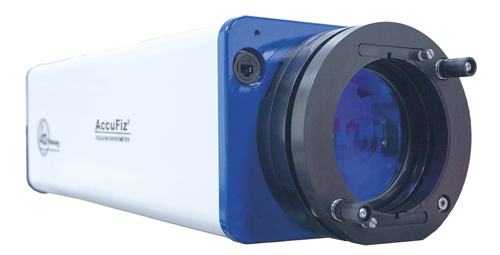
4D Technology recently developed and shipped what it believes to be the first continuous zoom Fizeau. Credit: 4D Technology
However, in the earlier designs, there was a drawback in the initial off-the-shelf zoom lenses integrated and used in an incoherent imaging configuration. They were acceptable for use with video cameras, but the company feels that in a Fizeau, they degraded the optical resolution of the imaging path of the instrument, resulting in a blurred image. When the available pixel density of the implemented cameras was SVGA or less, these zoom lenses were a good compromise. However, with the advent of megapixel and larger detectors, the situation changed. The early implemented zoom lenses were even less acceptable.
Image quality
‘As alternatives,’ explained Martinek, ‘manufacturers sometimes offered Fizeaus with a few fixed-focal-length (FFL) positions, where the interferometer was acceptably precise at discrete magnifications. Others offered digital zoom, a technique of enlarging the sensor image to fill the field of view, but without changing the focal angle of the optics. These alternatives’ imaging quality and ability to measure mid-spatial frequency features, exceeded the capability of systems with optical zoom. But you couldn’t get a true continuous-zoom Fizeau, varying the focal length infinitely along a range.’
Earlier this year, however, 4D Technology shipped what it believes to be the first continuous zoom Fizeau ever made. ‘Optical zoom means the image magnification is changed before it reaches the sensor,’ explained Martinek. ‘You can get great measurements, using magnifications from 1X to 6X. By using the internal optical zoom capability to more fully frame your optics, you maximise your datapoint resolution. Or, use the zoom to see features in greater detail, ending the myth that it was impossible.’
The dynamic interferometry technology referred to by Martinek is one technology pioneered by the company, which enables complex testing without vibration isolation, even in noisy environments. It allows for measurement between multiple tables, in environmental chambers, over long paths or in noisy cleanrooms. Polarisation is used to encode the test and reference beam. A proprietary, high speed, high resolution wavefront sensor enables all measurement data to be acquired simultaneously and quickly, in as little as 30 microseconds.
Widespread use
Dynamic interferometry technology is used today in a number of industries to provide accurate shape and surface measurement data, which provides feedback to customers of optical quality, machine finish, and surface defectivity, to improve manufacturing yield and performance. This technology became so sought after that advanced process control systems supplier, Nanometrics, has added it to its own portfolio, after purchasing 4D Technology, which was completed in November.
Dr Pierre-Yves Lesaicherre, president and chief executive officer of Nanometrics, explained: ‘The addition of this business and technology to Nanometrics enables us to serve new markets in advanced process control metrology and inspection. In addition to expanding our served markets, 4D’s technology enables next-generation systems for leading semiconductor device applications and is a natural complement to our current optical metrology and inspection solutions.’
The acquisition agreement of 29 October was closed on 15 November, with Nanometrics acquiring all outstanding shares of 4D Technology. The 4D Technology operation will continue in Tucson, Arizona, and the products will continue to be sold with the 4D Technology brand. Lesaicherre continued: ‘We are very pleased that the 4D Technology team is now part of Nanometrics.
'The addition of 4D Technology adds unique technology to our portfolio, expanding our served market with new applications in the scientific research, aerospace, industrial and optics manufacturing markets.’
Top image: Lab-on-a-chip is an example of a direct application dealing with the flow of liquids inside micrometre-sized channels.