The global semiconductor industry is set to grow by $90.8bn from 2020 to 2024 according to a report, with one of the biggest drivers being the use of semiconductor packaging technology.
Research firm Technavio’s forecast would demonstrate a 4 per cent CAGR over that time. But, with hundreds of steps over several weeks involved in the manufacturing process of semiconductor wafers, this particular growth does not come without its challenges.
Should there be any defects early in the process that are missed, then all of the subsequent time and cost-heavy work will have been in vain.
According to Jean-Francois Pichot, sales director at 3D measurement system provider Precitec: ‘The goal for these companies is to avoid producing bad parts. To do this, they need to undertake a quality inspection to avoid losing time and money caused by bottlenecks,’ he said.
‘In the semiconductor industry, time really is money. The more wafers they make per hour, the more revenue, and the materials they use are extremely expensive, so they do not want to have to scrap bad parts.’ That is why optical metrology equipment is now an essential tool in semiconductor production.
The little things
According to the Institute of Electrical and Electronics Engineers (IEEE), device feature sizes are projected to decrease to less than 5nm in the next two years. This means, said the IEE in its International Roadmap For Devices And Systems: ‘Scaling as we know it is expected to soon reach its physical limits, or get to a point where cost and reliability issues far outweigh the benefits. The use of complex 3D structures fabricated using new materials and processes with ever decreasing dimensions is also projected to accelerate within the next years.’
This means that metrology solutions must continually evolve and develop to accommodate an increasingly wider variety of technologies, said the IEE. What’s more, because instruments routinely measure near and at atomic scale dimensions, their manufacture requires an understanding of these materials’ properties and of the physics involved in making the measurement. And it’s not just the instrument manufacturing process that needs to adapt, as the test, measurement and monitoring of semiconductor production using different materials will also require different standards.
The European Metrology Programme for Innovation and Research (Empir) was developed as part of Horizon 2020, the EU framework programme for research and innovation. It has been funded by members of the Euramet alliance, to support collaborative research between measurement institutes, academia and industry to address key challenges and ensure measurement science meets the future.
The alliance’s A new standard for better 3D chips highlighted that, to address the nearing limit of processing power and demand for smaller devices, manufacturers are assembling chips with parts on top of each other, or stacking. This additional level of architecture, of course, requires new types of measurement, for instance, to verify that components are correctly aligned for devices to function.
In a case study published last year, Euramet explained that, while optical analysis methods currently offer the best solution, the standards required for accurate measurements at this nanometre scale are not yet available. So, under the Empir project, the National Metrology Institute of Germany (PTB) developed a standard using advanced electron-beam lithography and reactive ion etching techniques to enable a state-of-the-art characterisation of 3D microscopes.
The surface features nanometre sized, sharp-edged, circular concentric ‘rings’ made to precise dimensions with known measurement, the spacing, or distribution frequency, between each groove forms a geometric pattern that the PTB termed a ‘chirp’. The pattern is designed to be ideal for characterising a microscope’s instrument transfer function, which indicates the lateral resolving power of optical instruments for making 3D surface measurements. The rotational symmetric patterns of the rings are designed to detect angular-dependent asymmetries, and their depth informs an instrument’s performance at detecting the height of nanometre-sized structures, allowing optical measurements to be accurately assessed at the nanometre scale.
After the project optical measurement systems provider Zygo used the standard to assess the performance of its product range, including 3D microscopes, sensors and precision optical components. With its Nexview advanced optical surface profiler, the company was able to measure the new standard’s challenging features within the specified accuracies.
Semiconductor manufacturers benefit from completely non-contact optical metrology equipment to reduce the chance of a sample being damaged (Zygo)
The Nexview 3D imaging and measurement system was designed to provide interactive surface metrology for semiconductor analysis, with multiple measurements including flatness, roughness, large steps and segments, thin films, and steep slopes, with features’ heights ranging from <1nm up to 20,000µm. It features ISO 25178 surface measurement parameters and a streamlined design with no manual controls.
Zygo believes that the use of the standard helped the company improve the results of fine-structure surface measurements. Product manager Eric Felkel said: ‘Increased measurement precision for high-aspect-ratio components will allow a greater confidence in the use of optical microscopes for the rapid, inline detection of defects in 3D chips, as well as in other industries that use submicron components.’
Close collaboration
In the development of optical metrology systems for semiconductor production, it is important for providers to work closely with customers to understand their changing requirements. This is something Precitec’s Pichot believes is vital. ‘OEM customisation is very important to us. We work with customers and can customise a probe to adapt to the customer and their requirements.’
In terms of the types of technology available, Pichot explained that this is dependent on the stage of the production process. ‘There are basically three main stages,’ he said. ‘The first is the front end, where the wafer is prepared for manufacturing, so the functions are built up into the chip. Then, at some point the wafer is divided into small components, and then there is the packaging stage. That becomes a critical component, so they need very different, but always robust, sensors that can be integrated into each stage of their production processes.’
In each stage there are many smaller steps. At the front-end of production, for instance, comes photolithography, which allows the specification to be provided to the chip, which is then polished and brought to the correct thickness. This is a crucial point when it comes to optical metrology. ‘The thickness of the wafer needs to be monitored in-process,’ he said.
To save production time and prevent errors, ideally this needs to be an automated process, Pichot added. ‘If an instrument does not have sensors that can tell you at any time the thickness of the wafer, then the process will involve grinding, with breaks to check from time to time,’ he said.
Without in-system programming, the manufacturer might miss the target thickness they need to reach. ‘By using sensors like ours, grinding can be much more efficient because they can tell, at any time, the thickness. Only in the last minutes of the process does the grinding speed need to be reduced to get the right value,’ Pichot said. This can help to ensure that the product quality is more accurate and repeatable, but also offers the additional benefit of reduced material waste.
Advances in optical metrology allow for non-contact inline inspection with resolutions up to 1µm (Pretitec)
During photolithography, micrometre-accurate alignment of the mask and wafer is essential. One method is to use two or three chromatic confocal and interferometric non-contact detector probes to change the levelling of the wafer to ensure that it is the correct flatness before the photolithography process. ‘Specialist probes can measure the very thin layers on top of the wafer, to find the position of the wafer surface and separate the top surface to the wafer surface. It can be achieved down to one or two microns,’ explained Pichot.
A further challenge for semiconductor manufacturers when it comes to thickness verification is an increased market demand for wafers with ever-lower total thickness variation (TTV) or defined structured surface. The challenges lie in varying wafer thickness ranges, differing prime wafer materials, as well as what can often be a harsh inline process environment – for example, if there is no clear view of the wafer because of grinding sludge.
‘With TTV, a wafer, after being processed, might see some variation of signals from one side to the other,’ Pichot said. ‘With a sensor, you can measure the signal just from one side with super-high accuracy and map signal distribution. It can tell you “it is thinner here, but thicker here”, because it can check that the thickness everywhere is inside the specifications.
‘We also developed a powerful scanner for extremely fast measurement of this thickness variation, because the wafer does not need to be moved underneath the sensor. Mapping can be achieved accurately, and provides thickness, but also information about what we call the bow and warp – the shape of the wafer in one single pass. It’s time-saving for the customer.’
A polished finish
Advanced optical metrology equipment can also be used to provide preventive maintenance during the polishing process, noted Pichot, as it can help determine the degree of surface wear of the polishing pads, caused by what can be quite a harsh process. ‘The polishing pads are in contact with the wafer during the polishing process and after hours of activity, those pads wear down until they need changing. By incorporating a sensor directly inside the brushing machine the depth can be measured of the segments in between the pads, so the instrument can light up to tell the user the pad needs to be replaced.’
A specifically-designed quality inspection service can be very useful when it comes to defect detection such as chips or cracks that can occur when the die is separated from a wafer of semiconductor (dicing). Dicing is usually performed by scribing, breaking, mechanical sawing or laser cutting. ‘For fast and accurate solution,’ said Pichot, ‘optical sensors can be used to check the roughness of the wafer nanometric scale. We can measure the depth after the use of the laser. For example we can detect with advanced microscopy problems like cracks in the wafer. Sensors can also check any photo-resistant coatings that may have been applied to a wafer, have been removed without causing damage.’
With so many steps involved in the manufacture of semiconductors, and with new materials being introduced all the time, there is an almost non-exhaustive list of applications for which optical metrology is essential.
Other applications include the measurement and inspection of wafer-level and solder; die and wafer bonding; the inspection of probe cards and even measurement of the tiny wire bonding that connects the chips to the package. ‘In the semiconductor industry, we have a lot of customers, and therefore a lot of interesting applications,’ said Pichot. ‘Once we get started, it really is quite fascinating, the number of things we can achieve.’
Sponsored: LBP has the measure of mirrors and optical components
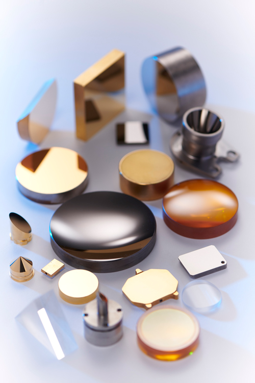
As an optical manufacturer it is essential for us to be able to measure all the optical properties of a lens or mirror before sending it out to the customer. We regularly provide sub micron measurements on our mirrors and optical components, so need to ensure that we have the necessary metrology and expertise in-house.
We use a variety of equipment and measurement techniques, depending on the specification of the optical component.
Laser calorimetry
We use laser calorimetry to determine how much heat will be generated in an optic when a high-power laser beam is passed through it – to give a measure of the ‘absorptance’ or ‘absorption’. Too much heat and the optic can change its properties or even be damaged.
Using an in-house design, the measurement involves exposing the optic to a laser beam and recording the temperature rise, followed by the subsequent temperature drop after the laser is switched off. The temperature sensor is a thermocouple connected to an amplifier and logged by a computer. The rate at which the temperature rises tells us the rate at which laser power is being absorbed, and the cooling rate tells us how quickly the optic is losing heat to the surroundings – which is also happening during the heating stage. With a knowledge of those heat gain and loss rates, the laser power and the heat capacity of the optic, the absorption can be calculated, usually expressed as a percentage.
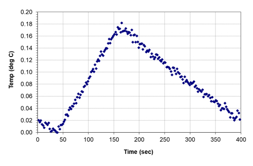
Temperature vs time during an absorption measurement of a ZnSe high-gas pressure lens with absorption of 0.16%; initial cooling, laser heating and final cooling
Interferometry
The specifications of most optical mirror surfaces involve sub micrometre dimensions, too small to measure mechanically. For the majority of our optical mirrors we use a phase shifting interferometer for quality assurance. With software analysis of the interference pattern, a hard copy of the results is available to our customers. This demonstrates that surface form specifications such as power and irregularity have been met. We also use interferometry to measure the wedge of flat laser mirrors to ensure parallelism.
Interferometry is useful to measure and align optical assemblies such as reflective beam expanders or collimators, with an interferometer. We have investigated the mounting of optics, observing the deformation that can occur to mirrors from poorly designed mounts or excessive mechanical force. We can supply mirrors complete with mounts and internal water cooling, proven by interferometry that the assembled mirror has not been deformed.
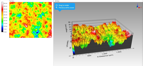
3D optical profiler
Our 3D optical profiler (Filmetrics Profilm 3D) uses state-of-the-art white-light interferometry to enable us to measure surface roughness from sub-nanometre to millimetre scale – something that is essential for some of our customers, where surface finish is vitally important. Reports are easily generated and can be supplied upon request.
Analyser used for mirror phase retardation
We also use a Brewster plate attenuator – normally used to attenuate a linearly polarised laser beam – as an analyser to assess the polarisation of a laser beam. The Brewster plates will require an ‘enhanced’ coating on one side, this increases the maximum attenuation (reduces minimum transmission) considerably. The attenuator then behaves very much like a linear polariser, closely following Malus’s law with transmission T = cos2θ, θ being the angle between the direction of polarisation and the transmission axis of the analyser/attenuator.
Used with a CO2 laser, these Brewster plates are made from ZnSe and are tilted in a ‘V’ configuration at 67.4° incidence angle, as shown below.
To check the phase retardation produced by a mirror, the analyser is rotated in the reflected beam and transmitted power measurements recorded with angle.
For example, if the test mirror is a ¼-wave phase retarder, the reflected beam will be circularly polarised, and the power measured will be the same at all angles.
Optical surface form measurements
Now that optical designers are becoming more aware of the capabilities of modern day machine tools, they are increasingly using torics, cylinders and other non-rotationally symmetrical surfaces in their optical designs. It has become increasingly important for our diamond machining division to give our customers and engineers confidence that all drawing specifications have been met.
The Form Talysurf PGI optics contact stylus optical profilometer, when equipped with an additional “Y” stage, is capable of measuring these advanced surfaces in X Y Z – such as spherical, diffractive, fresnel and aspheric lenses. The data is used to produce a three-dimensional map of the generated surface and calculate any deviation from the design specification.