Hamamatsu Photonics is certainly one of the photonics industry’s big hitters. With an €800m turnover, more than 4,000 employees worldwide and numerous offices and subsidiaries around the globe, it’s a serious player – with products across the photonics spectrum, from detectors and diodes, to sensors and light sources and beyond.
Originally founded in Japan in 1953, Hamamatsu initially focused on the development of electron tube products, primarily photomultipliers, based on their glass and vacuum technologies. Over time, the company’s product range increased enormously to include light sources, opto-semiconductors, silicon photodiodes, CCD technology, infrared detectors and more.
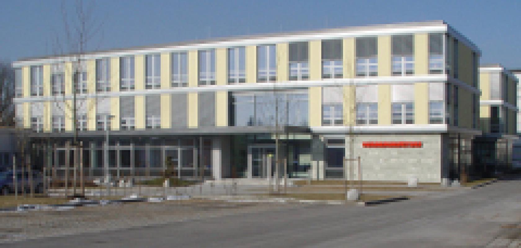
The name Hamamatsu formally hit Europe in 1973, with the founding of the first European subsidiary, Hamamatsu Europe. It was later renamed Hamamatsu Photonics Germany, as other subsidiaries were started throughout the continent in France, UK, Scandinavia and Italy. Dr Peter Eggl is managing director of the recently-formed Hamamatsu Photonics Europe, and also serves as managing director of Hamamatsu Photonics Germany, a position he has held since 1993. He originally joined Hamamatsu in 1987, having used the company’s products during his time studying for a PhD in physics at the University of Munich. ‘Having been impressed by the products, when I finished my studies, I thought Hamamatsu would be an interesting company to join,’ says Eggl. This he did, initially as a sales engineer.
‘In Europe, our main business is in optoelectronic components,’ says Eggl, ‘although we also have some system-oriented business. We also have very good relationships with other manufacturers of photonic equipment. Many manufacturers of analytical or spectroscopic devices are using our detector technology.’
Just as important as the range of technology available is the variety in applications that it serves. ‘A large quantity of our products end up in the education and research sector at universities,’ says Eggl, ‘where they are used mainly by physicists and electronic engineers. More than 50 per cent of our staff have strong academic and technical expertise in a wide range of disciplines such as physics, life sciences and electronics. We are therefore in a strong position to be able to support and understand the technical needs of these diverse application areas.’
‘Historically, our main applications have been in the analytical area, but during the past 10 years we have seen huge growth in other markets. In the medical area, for example, our products are increasingly used for x-ray imaging, in particular for medical CT and dental imaging.
‘We are also involved in PET (positron emission tomography) medical scanners, and are developing new techniques such as their use in conjunction with NMR (nuclear magnetic resonance) to produce highly-detailed images to provide medical teams with a much better understanding.’

Dr Peter Eggl, managing director of Hamamatsu
The automotive market has also grown in recent times, in particular with the use of the plastic fibre optical data bus (so called ‘MOST protocol’), which is used to connect GPS, telephone, CD players, radio and so on, in place of copper wires. ‘This technology requires an emitter and a photo IC for detection, which we supply,’ says Eggl. ‘Previously, this was a relatively low-volume business as it was only ever used on high-value cars, but it has now entered the mass market. Similarly, with European concerns over emission targets and the introduction in 2014 of the Euro 6 Regulation, we believe optoelectronic components can play a big part in reducing emissions from vehicles in the years ahead.’
Hamamatsu’s products have also been finding their way into a large number of industrial applications, and this encompasses a broad range of markets, including non-destructive testing. ‘In the food industry, for example, our detectors help check containers for contamination via x-ray,’ says Eggl. ‘PCBs are also inspected via x-ray – and, in the wood industry, the technology is used to check for defects in the wood itself.’
The majority of Hamamatsu’s manufacturing is carried out in Japan, where it has three closely located sites in and around Hamamatsu City. There is a further manufacturing facility in China, which deals with photomultiplier technology. Hamamatsu is 500km from the site of the recent incident at the Fukushima nuclear power plant, so was largely unaffected in terms of operations (though a statement on its website expresses sympathies to all those who were affected, and Hamamatsu Europe has pledged support to the recovery effort).
There are 15 offices in Europe, representing a turnover of around 220m euro, and containing 200 staff, who deal with sales and marketing, as well as service, support and installation. In October 2010, Hamamatsu Photonics Europe was created to bring together some core functions across these 15 offices. ‘We’re looking for synergies on, for example, marketing issues,’ says Eggl, ‘as well as IT, finance, human resources and, to some extent, service and support. This will enable us to provide both the highest level of customer support and a “global” response to our international customers.’
The company managed its way through the financial crisis relatively unscathed, with its European operation suffering a mere five per cent dip in sales, although some markets were obviously hit harder than others. ‘Although markets such as automotive dipped greatly, we were able to compensate for this by finding new applications,’ says Eggl. ‘Since then, we’ve enjoyed a very successful period, and we are expecting sustained growth in coming years.’
So why should customers choose Hamamatsu over its competitors? ‘The key for Hamamatsu is that we have a high concentration of optoelectronic technologies,’ says Eggl. ‘There is no other company that has so many technologies in-house. We are able to produce any kind of optoelectronic detector ourselves. Our products also offer very high quality and reliability. What is also important for many of our customers is that we have a long product lifecycle. Not only does this guarantee long-term availability of replacement parts or complementary products, but it also means that for those in the medical industry, they will not have to go through the FDA approval process again, which can be required even if just one component changes. This is time-consuming and costly, as you can imagine.
‘Our customer service and the reliability of our deliveries also ensure repeat business for us. We have a positive mid- to long-term strategy too. Around 10 to 15 per cent of our global revenue is reinvested in R&D, so we are continually looking at new products. We also maintain a close relationship with academia, so we know what is going on from a research perspective. Europe, for example, is leading the way in high-energy physics research, where our custom-made products can be found in the particle accelerator at CERN, for which we received many accolades and awards.’