The global diffractive optical elements (DOE) market is booming, with an estimated revenue growth of just under 7.5 per cent during 2018, according to a report from Persistence Market Research. This growth is likely to exceed $500m this year. The report highlights more market opportunities are likely with improving investment in R&D, in particular in the work of universities in micro-optics.
As well as advancing the adoption of micro-optics in many applications, print-optical technology is serving a vital role in shaping the overall demand for DOEs, as the growing use of 3D printed micro-optics is enabling more manufacturers to deliver customised micro optic products.
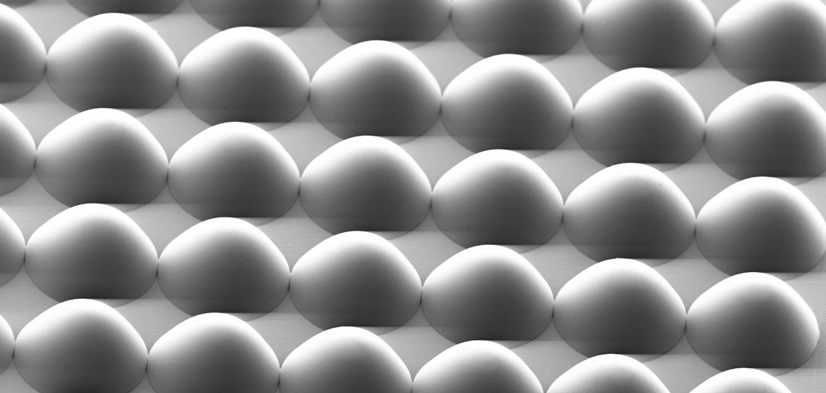
A number of new developments in this area were shown at the recent Laser World of Photonics. One was the Quantum X two-photon grayscale lithography system from 3D printing firm Nanoscribe. The device is designed for the maskless lithography of highly precise micro-optics in response to demand for high-throughput manufacturing, for example, in the sensors, mobile device, data and telecommunications sectors. Using two-photon grayscale lithography (2GL) printing technology combines the performance of grayscale lithography with the flexibility of two-photon polymerisation for a number of uses.
The Quantum X is equipped with three live-view cameras for process control and a resin dispenser. To simplify the change-over between hardware configurations, objective and sample holder recognition run automatically. Multi-level DOEs can be produced by modulating the laser power in one scanning plane, reducing the print time necessary for multi-layer microfabrication.
Making shapes
Refractive micro-optics also benefit from the contouring capabilities afforded by 2GL processes, making single optical elements, arrays with high fill factors of up to 100 per cent and varying shapes such as spherical and aspherical lenses possible in a maskless process. A system such as the Quantum X can fabricate almost any imaginable 2.5D shape on the microscale, which the company says will pave the way to new or strongly enhanced optical elements from imaging, to illumination or sensing.
Martin Hermatschweiler, CEO of Nanoscribe, said: ‘The developers have put great effort to excel in advanced user–machine interactions. For example, users can check on the job status, adjust process controls and visualise printing in real time, directly on the built-in touchscreen. To manage and organise the users’ projects, a continuous execution of a series of print jobs is supported by a job queue. Using two-photon grayscale lithography, high-precision components materialise with excellent shape accuracy and ultra-smooth surfaces, thanks to the contouring capabilities of the 2GL voxel size control. Laser power modulation and dynamic focus positioning are synchronised accurately at high scanning speeds, enabling full voxel size control along each scanning plane.’
Using a fabrication process in this way allows a wide range of substrates – including transparent and opaque ones – accepting sizes of up to six-inch wafers, and can avoid costly mask fabrication, spin-coating and pre- or post-baking when used with photo-resin materials. The device made quite an impact on its launch at the Munich trade fair, picking up an Innovation Award on the first day of the show.
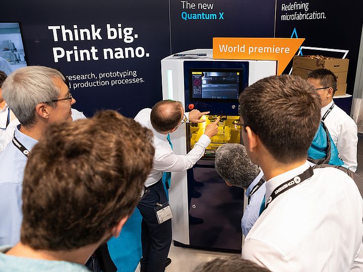
Demonstration of the Quantum X at Laser World of Photonics in June. Credit: Nanoscribe
The prize, sponsored by the publishers of Electro Optics, was presented to Nanoscribe after it was selected by a jury made up of the heads of the Optical Society, Spectaris and Toptica among others. Hermatschweiler said: ‘After a very intensive technical development phase, this is a great recognition for our team and for the outstanding performance of our new maskless lithography system Quantum X.’
Face to face
For Dirk Hauschild, CMO at optics manufacturer Limo, innovations in micro-optics have been taking place for some time, but today there are more varied applications for which they are used. ‘The latest surprising device using micro-optics,’ he said, ‘is the face ID from Apple. Then, there are time-of-flight measurement cameras on smart phones from manufacturers throughout the world that use laser illumination for 3D sensing. For consumer applications, this is the breakthrough in using not only normal optical elements for imaging, but using lasers in combination with micro-optics that shape the light – that really enables these applications. This was, I think, the most prominent example of using micro-optics in the last three years.’
Hauschild also pointed to autonomous driving as one huge application that will drive growth in the micro-optics sector. ‘A laser illuminated area can, together with a camera, detect the distances between objects and the car. In the current applications, the sensor in 3D sensing is something that opens new machine-human interfaces to get access to machines. For example, cars will get 3D sensors that only start the car if the right person is in front of the steering wheel. The micro-optics really enable, or are the missing link between, the light source and the application.’
Similarly, said Hauschild, in China there are hotels that use laser illumination and cameras to detect 3D images from a face, like a finger print for check-in purposes. ‘That’s really booming, and there are companies in China making developments in this direction. It is fascinating how they produce and assemble half a billion optical components a year. This is the low-end field of application – so low power and low cost, but high quantities. Limo is a small to medium company, so typically we are in the range of 100,000 to a million pieces.’
Under control
A key focus for Limo is to use micro-optics for high-power laser applications to enable the laser source to be transformed into a precision tool. ‘Light is the purest form of energy,’ Hauschild said, ‘so, if you can control the light, you can control all the processes and you can bring the light with light speed to the application. If you have the right beam shape, finally, the application will run much better than without beam shaping.’
At Laser World of Photonics, the company introduced new micro-optics for the production of flexible OLED displays. The sGauss beam profile features steeper edges, improving the throughput of UV lasers used in OLED manufacturing. ‘We changed the beam profile into new geometry,’ explained Hauschild, ‘and with the same laser power we increased the productivity up to 30 per cent.’
The optical design was enhanced far enough that the Gaussian profiles can be turned into a line with a length of up to 1,000mm and a width of 30µm. The steeper edges allow the laser energy to be used more effectively to separate the display film, and laser lift-off (LLO) process productivity can be increased by more than 30 per cent. The micro-optics for the sGauss profile are modular and feature a continuously adjustable line length and width. Existing systems can also be retrofitted with a sGauss module, allowing manufacturers to either directly boost productivity or, where less laser energy is used with the same systems, significantly extending the service life of their lasers. This new technology will also unlock other applications for UV solid-state lasers, such as annealing and crystallisation.
Hauschild said: ‘After the [Laser Munich] show, some of the display makers came to us and gave us samples, and for some special materials we increased the productivity by 80 per cent. This was surprising. If you optimise the material and processing beam shape, we can bring the laser material processing to a much higher level of process efficiency than with a non-optimised beam profile.’
Micro-optics are not without their challenges, and for Hauschild ‘one of the biggest challenges, every day, is to deliver the highest quality for the lowest price’. He said: ‘We must also convince our customers that optical glass elements have a value that gives them the possibility of a very safe operation for many years. Finding the sweet spot of performance and price is challenging. If you scale the highest quality to large quantities at the end, you have to reduce the quality to optimise the cost and the price structure. It’s about finding the right ratio of price and performance.’
Speaking from experience
The other challenge, he said, is the level of knowledge and experience in micro-optics. ‘Some of the companies that want to buy the optics, even today do not have enough experience in how to make use of all the advantages of the micro-optics’ functionality in the market. It means we often get enquiries asking us to produce a compact optical device, but they have no idea how to design the small optical system. There are only a few specialist companies in the world that have experience in how to design compact optical systems in a way that you get a good price performance ratio.
‘The major difference between micro-optics and optics, is that in micro-optics you have not only one or two curved surfaces, but a variety of optical and mechanical surfaces for easier integration into optical devices. That’s more complicated, in terms of design and assembling, but it simplifies the optical set-up, and micro-optics is still not something that you can study at university. I don’t know why. In Germany we have some institutes that offer this course of training in small optics, micro-optics and all the benefits, but this is not the standard. The standard is technical optics in general, that means all the equations that the physicists developed more than 300 years ago.’
Looking ahead, Hauschild believes that, while there may not be many opportunities to make improvements in the technology, new applications for its use will continue to present themselves. ‘Moulding is also a technology to replicate a master structure using liquid glass, so this also opens the field of free-form optics. This means you can make one sophisticated tool with a crazy shape, and then you replicate it into glass just by pressing this master structure into the liquid glass, so that it’s heated up to 600-700 degrees. This has good possibilities for use in free-form shapes with multi-functional surfaces, but it is limited, in terms of applications with high added value.’
At the higher end of pricing, Hauschild said there are unlimited uses, with small and medium quantities up to tens of thousands of pieces. ‘Applications with polymer lenses seem almost unlimited,’ he said. ‘It’s a question of how open you are to designing new optical systems. Augmented and virtual reality glass are still at the beginning, the question is how to come to the right price level or the right features that people really want. Maybe Microsoft HoloLens and Google activities, with a lot of micro-optic components are a good example, but people are not open to pay $1,000 for such a gadget.’
Hauschild believes the era of highly integrated micro-optics will come. ‘So many industries use optics in a more traditional way, and adding the features of micro-optics, beam shaping and shaping pictures – making something more compact and lightweight and combining functions in one optical element – it’s a never-ending story. This is because we are, every year, still at the beginning.
‘There are so many applications coming. We have made a lot of steps forward but in many applications, the cost structure from high-end to low-cost consumer applications, for example, will open a lot of new possibilities. In industrial production, for example, people are starting to use micro-optics in a smarter and more efficient way.’ EO