In the ranks of 21st-century wonder materials, photonic crystals are right up there with graphene and room-temperature superconductors as the ‘next big thing’. Common enough in nature – think butterfly wings, peacock feathers, or the shimmering colours of opal – they have been proposed as the secret behind such outlandish technologies as invisibility cloaks and tricorder-style nanofluidic biosensors.
One of the most promising applications of photonic crystals remains in computing, in particular as a key component in quantum computing. It has been seven years since the first solid-state quantum processor was built at Yale, and six years – long enough for Moore’s Law to deliver an eight-fold increase in silicon chip complexity – since the first demonstration of a quantum computer by researchers at Humboldt Universität in Berlin. That was a pretty rudimentary affair, using electronic excitations in nano-diamonds as qubits and photonic crystal optical nanostructures. While progress is certainly being made, practical applications of quantum computing – such as next-generation cryptography – still seem like science fiction.

Once the laser beam hits the surface of a sample it starts to generate heat, which not only diffuses along the membrane, but also diffuses to the ambient gas. This effect reduces the width of the temperature distribution in the photon. (Credit: University of Twente)
Photonic crystals get their optical properties through a structural arrangement on the scale of hundreds of nanometres – the same range as optical wavelengths. A crystal may be synthesised to transmit light of a particular wavelength while blocking others, allowing them to act as filters or waveguides. 2D photonic crystals can split a light source into different wavelengths, with applications in optical communications and other fields, while 3D crystals can trap and release photons to make them analogous to transistors in an electronic circuit.
Turning these intriguing properties into affordable functional processors is a major ambition of the computer industry, as it seeks ways to overcome the limitations of silicon-based semiconductors. Optical chips look like the only way to make quantum computing a reality, exploiting the bizarre qualities of photons to appear in more than one place and state at the same time. Where an electronic computer relies on the familiar 1 or 0 states of a digital bit, a quantum bit (qubit) can be 1 or 0, or both, or neither, and can be entangled at a quantum level with another photon.
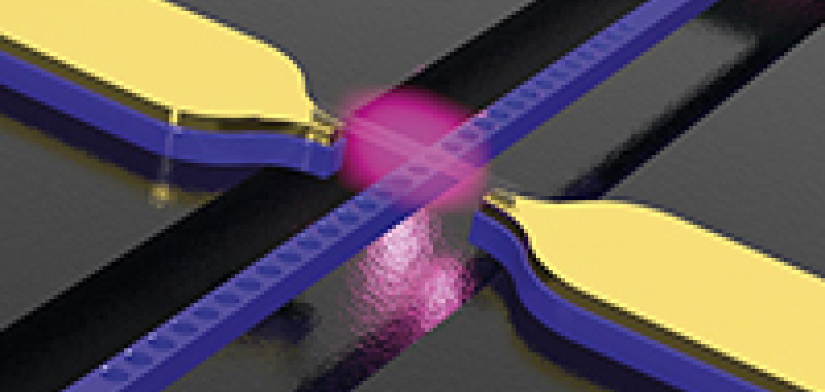
In April 2016, researchers at Karlsruhe Institute of Technology (KIT) demonstrated that carbon nanotubes can be used as an on-chip light source for photonic circuits. Recording their findings in Nature Photonics, they reported that carbon nanotubes about 1,000 nanometres long, and only one nanometre in diameter, can be integrated into a nanostructured waveguide. This creates a miniature switching element which converts electronic signals into clearly defined optical impulses.
The nanostructures act like a photonic crystal and allow customising of the properties of light’ explained authors Felix Pyatkov and Valentin Fütterling. The nanotubes generate light of the desired wavelength within a tightly controlled band, and these novel light sources can be integrated into highly complex structures, they added. The structures produce photons ‘about as strongly as a laser’ when an electric signal is applied, and respond at high speed to variations in input signal. These optoelectronic components have been used to create light signals in the gigahertz frequency range.
Generating the light in a photonic circuit is one thing, but manipulating and controlling it is another issue altogether. The classic way of doing so is through the application of heat, to change the properties of circuit components. But heat has a tendency to diffuse and, as a consequence, neighbouring elements will also be affected and may undergo unwanted structural changes.
Scientists from the MESA+ Institute for Nanotechnology at the University of Twente, Netherlands, and Thales Research and Technology, France, reported a method for controlling heat propagation in photonic devices in the journal Applied Physics Letters (April 2015). They controlled surrounding or embedding media to provide an ‘extra degree of freedom’ to control the heat distribution in thin photonic crystal membranes.
The team showed that significantly better control is obtained if high thermal conductivity gases are used as the surrounding media. With helium, for example, the width of the temperature distribution in the structure is reduced by 30 per cent when compared to air. This, they say, enables thermal tuning of coupled resonators, which will be valuable in the quest to build programmable optical circuits.
A rather different approach has been taken by researchers at the University of Southampton, UK and the Institut d’Optique in Bordeaux, France, who have reported being able to control light in a photonic circuit through ‘spatial light modulation.
They set out to create reconfigurable optical elements as a step towards the ultimate aim of developing a field-programmable photonic chip. Traditional spatial light modulators are based on liquid crystals or micro mirrors, but these are dispensed in favour of multimode interference (MMI) devices. These are in common use for splitting and recombining signals on a chip, but have characteristics that are fixed at fabrication.
Writing in the journal Optica in April 2016, the scientists described how the ‘intricate interplay’ between the many light modes travelling through the MMI allows it to be controlled dynamically. A pattern of local perturbations, induced by a femtosecond laser, acts effectively to shape the transmitted light and allows it to be routed through a static silicon element. This in turn transforms the MMI into a building block for field-programmable photonics, they say.

Repeated etching and passivation produces spherical depressions to become the basis of novel waveguides. (Credit: Karlsruhe Institute of Technology)
Manufacturing photonic crystals
In the absence of a commercial photonic crystal mine, the growing use of crystals and the likely explosion in demand in the next few years means that much attention is being paid towards finding innovative ways to make them quickly and cheaply.
Conventional manufacturing involves defining a pattern in the photoresist, using a mask and UV light, then etching or depositing material layer by layer on a silicon chip substrate. The process is laborious and has many limitations, including restrictions on the number of layers that can be stacked.
An etching method called SPRIE (sequential passivation and reactive ion etching) was introduced for rapid cheap photonic structures, exploiting the self-organisation principle. Developed at Karlsruhe, it can produce a three-dimensional photonic crystal within a few minutes and, in principle at least, allows a three-dimensional structure to be generated using a freely choosable mask.

Teleportation crystals retain information about quantum states even after the photon is obliterated. (Credit: GAP, University of Geneva (UNGE))
Optical properties of materials can be decisively influenced by specific structurisation,’ said Andreas Frölich from KIT. Under the SPRIE method, a solution with micrometre-sized spheres of polystyrene is applied to the silicon surface. With drying, the spheres self-organise into a dense monolayer and a honeycomb etching mask remains on the silicon surface. ‘This is our two-dimensional template for the construction of the three-dimensional structure’, said Frölich.
The free areas are removed by etching with a reactive plasma gas, and an electric field is applied to make the gas particles etch into the depth. Repeated etching and passivation makes the holes of the etching mask grow as the depth builds. Instead of a simple hole with vertical smooth walls, every etching step produces a spherical depression with a curved surface to become the basis for the regular repeating structures of novel waveguides.
An alternative new method from the University of Twente’s MESA+ research institute enables large-scale production of photonic crystals and makes it possible to produce chips with additional functions, say its originators.
This potentially ground-breaking development builds a 3D nanostructure on a chip in a single process, rather than layer-by-layer. A special 3D mask defines the structure on two sides of the wafer simultaneously, ensuring that both sides of the chip are neatly aligned and guaranteeing the vertical alignment of the final 3D nanostructure. A limitation of multiple-deposition methods is that layers that are relatively far apart can become randomly displaced to one another, limiting the chip’s functionality.
The method, described in the journal Nanotechnology in November 2015, paves the way to the mass production of photonic chips for multiple functions. ‘Our method makes it possible to combine an endless variety of features on a chip, such as electronics, optics, magnets and microfluidics,’ said Professor Willem Vos of the Complex Photonic Systems group (COPS) at MESA+.
The researchers discovered the method while working to develop new types of photonic crystals. They have succeeded in trapping light in crystals with embedded cavities and controling the direction in which the light travels.

The MESA+ method makes it possible to define a 3D nanostructure on a chip in a single process. (Credit: MESA+ Institute for Nanotechnology at the University of Twente)
Teleporting to the future
The advent of photonic crystals in the everyday world could have as profound an effect on society as the arrival of silicon electronics a few decades ago, and could make today’s most powerful devices seem like quaint relics. More interestingly, completely new phenomena could become commonplace – such as quantum teleportation.
Already, the quantum state of a photon has been ‘teleported’ to a photonic crystal over a distance of 25km and there seems no obvious reason why any distance should be a barrier. Experiments like this, conducted at the University of Geneva in 2014, have confirmed the distinctly non-intuitive prediction of quantum physics – that it is not the composition of a particle that is important, but rather its state, and this can persist even outside extreme differences, such as those distinguishing light from matter.
Quantum entanglement involves two photons inextricably linked at a fundamental level, one of which is propelled along an optical fibre, while the other is held in a photonic crystal. In what the Geneva scientists describe as something like a game of billiards, a third photon hits the first and obliterates it, along with itself. In the quantum teleportation effect, this information contained in the third photon is not destroyed but rather it appears in the second entangled photon, trapped 25km away in the crystal.
Lead author Félix Bussières described the remarkable effect in Nature Photonics in September 2014: ‘These two entangled photons are like two Siamese twins, their quantum state is a channel that empowers the teleportation from light into matter’.
In other words, an item’s quantum properties transcend classical physical properties. In a world that is familiar with technologies like the electronic transmission of information over physical networks, these ‘spooky’ phenomena may take some time to get used to. But when we do, quantum crystals will be at the heart of many cutting-edge developments.
Conventional optical fibre endoscopes have proved revolutionary in the diagnosis of disease, and now the frontier is moving to super high-resolution instruments that can resolve the individual cells of living patients.

Electron microscope image of a photonic crystal fibre endoscope: the glass is black, the air is grey and the red dot illustrates the focus.
An advanced wavefront shaping method developed at the University of Twente makes it possible to focus lensless light at an unparalleled resolution, according to a report in Optics Letters in January 2016. The resolution of fibre endoscopes is one micrometre at best, and some endoscopes use a number of fibres which each act as a discrete pixel in the final image.
Alternative multimode fibres could offer much better imaging and still be as thin as a tenth of a millimetre. The trick is unscrambling the images received at the fibre end, which a team of scientists under the direction of Dr Lyubov Amitonova have shown can be done with the use of photonic crystal fibres.
Photonic crystal fibres act as multimode fibres, with the image scrambled by light bouncing off the irregular wall of the fibre. The technique of complex wavefront shaping is able to undo this scrambling – generating a sharp image – by pre-shaping the light before it enters the fibre.
Amitonova and her colleagues have shown that this wavefront shaping technique – together with a properly designed multimode photonic crystal fibre – allows the creation of a tightly focused spot at the desired position on the fibre output facet with a subwavelength beam waist. This paves the way towards high-resolution endoscopic imaging via fibre probes so thin that they could be inserted, for instance, into tiny blood vessels not much thicker than a human hair.
Crystals for high power lasers
The growth process of large single-crystal fluoride materials is being developed by Northrop Grumman Synoptics, a manufacturer of solid-state laser materials and components. The materials – intended for Faraday rotator/isolator applications – are a promising replacement for the standard terbium gallium garnet (TGG) crystals currently used. The growth and performance of these fluoride materials were discussed in Laser Technik Journal in May.
The paper acknowledged the recent improvements made to high-power fibre lasers, and addressed the need to develop alternatives to the TGG crystals commonly used alongside them. Although TGG provided superior transmission properties and an ability to form large crystals, defects would occur within the larger crystals that limited their overall transmission performance. The new material therefore had to be able handle the increasing power levels of fibre lasers, while exhibiting the useful properties of TGG.
In particular, two single-crystal fluoride materials showed promise for use with higher power lasers. Both lithium terbium fluoride (LTF) and potassium terbium fluoride (KTF) crystals exhibited transmission properties similar to TGG, and enabled the performance of optical isolators at power levels previously attainable only with significant design compromises. The authors of the paper concluded that their advancements in the growth of LTF and KTF crystals will lead to improved optical isolation performance for high power lasers.