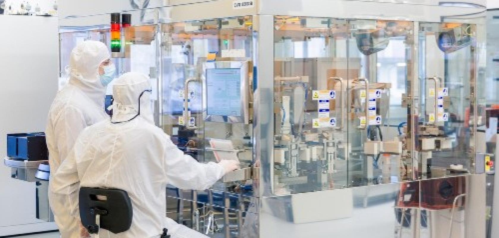
French research institute CEA-Leti has extended its 300mm silicon-based wafer line, opening it up for production of integrated photonic chips and III-V on silicon devices.
The announcement was made at the IEEE International Electron Devices Meeting, which took place from 1 to 5 December in San Francisco, USA.
The extension will allow new innovative technological modules to be inserted in, or made compatible with, industrial flows. Targeted technology includes edge AI, HPC, in memory computing, photonics, and power electronics.
CEA-Leti's CMOS strategy is based on a mix of priorities of CEA-Leti’s partners and its researchers’ ideas that pioneer enabling technologies to address societal challenges. These include cloud and edge computation, high-volume communication, multi-modality interaction and energy conservation.
‘Our 300mm line will help Leti continue this strategy by accessing dimensions that make it possible to address the pressing challenges associated with emerging technologies, such as quantum, nanowires and sequential 3D integration,’ said Emmanuel Sabonnadière, CEA-Leti CEO. ‘CEA-Leti’s industrial partners are now able to develop or test their disruptive technologies and their designs on state-of-the-art equipment, while benefiting from the institute’s R&D expertise, to achieve improved component performance, direct comparison with the ecosystem and easier technology transfers from lab to fab.’
The implementation of the 300mm line is possible thanks to financing of Auvergne Rhone Alpes region for the acquisition of a 193nm immersion lithography tool. CEA-Leti also benefited from financial support of the French government for the second phase of this plan (2018-2019).


