Researchers have developed an extremely thin chip with an integrated photonic circuit that could be used to exploit the so-called terahertz gap – lying between 0.3-30THz in the electromagnetic spectrum – for spectroscopy and imaging.
This gap is currently something of a technological dead zone, describing frequencies that are too fast for today’s electronics and telecommunications devices, but too slow for optics and imaging applications.
However, the scientists’ new chip now enables them to produce terahertz waves with tailored frequency, wavelength, amplitude and phase. Such precise control could enable terahertz radiation to be harnessed for next-generation applications in both the electronic and optical realms.
The work, conducted between EPFL, ETH Zurich and the University of Harvard, has been published in Nature Communications.
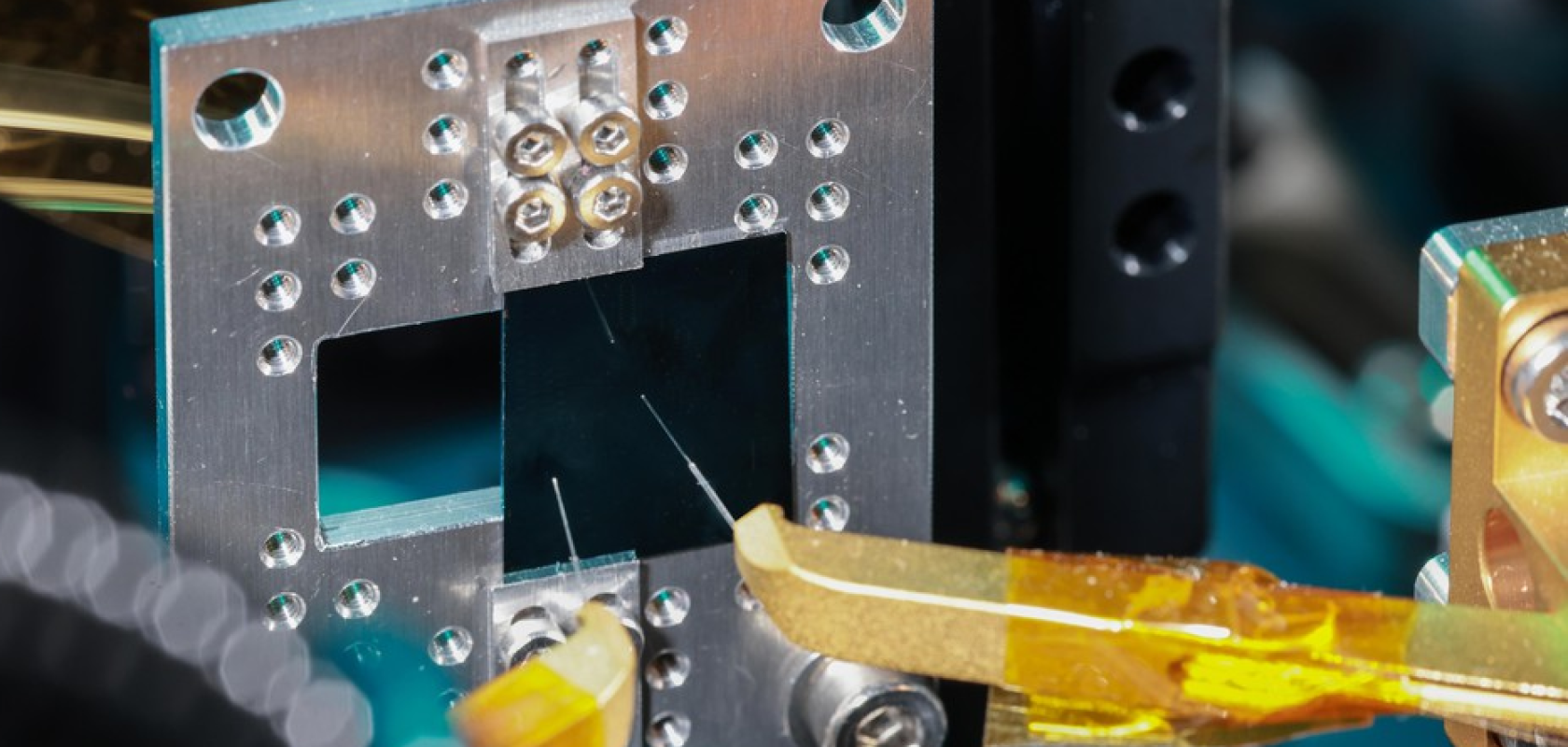
Cristina Benea-Chelmus, who led the research in the Laboratory of Hybrid Photonics (HYLAB) at EPFL’s School of Engineering, explained that while terahertz waves have been produced in a lab setting before, previous approaches have relied primarily on bulk crystals to generate the right frequencies. Instead, her lab’s use of the photonic circuit, made from lithium niobate and finely etched at the nanometre scale by collaborators at Harvard University, makes for a much more streamlined approach. The use of a silicon substrate also makes the device suitable for integration into electronic and optical systems.
“Generating waves at very high frequencies is extremely challenging, and there are very few techniques that can generate them with unique patterns,” she explained. “We are now able to engineer the exact temporal shape of terahertz waves – to say essentially, ‘I want a waveform that looks like this.’”
To achieve this, Benea-Chelmus’ lab designed the chip’s arrangement of channels, called waveguides, in such a way that microscopic antennas could be used to broadcast terahertz waves generated by light from optical fibres.
“The fact that our device already makes use of a standard optical signal is really an advantage, because it means that these new chips can be used with traditional lasers, which work very well and are very well understood. It means our device is telecommunications-compatible,” Benea-Chelmus emphasised. She added that miniaturised devices that send and receive signals in the terahertz range could play a key role in sixth generation mobile systems (6G).
In the world of optics, Benea-Chelmus sees particular potential for miniaturised lithium niobate chips in spectroscopy and imaging. In addition to being non-ionising, terahertz waves are much lower-energy than many other types of waves (such as x-rays) currently used to provide information about the composition of a material – whether it’s a bone or an oil painting. A compact, non-destructive device like the lithium niobate chip could therefore provide a less invasive alternative to current spectrographic techniques.
“You could imagine sending terahertz radiation through a material you are interested in and analysing it to measure the response of the material, depending on its molecular structure. All this from a device smaller than a match head,” she said.
Next, Benea-Chelmus plans to focus on tweaking the properties of the chip’s waveguides and antennas to engineer waveforms with greater amplitudes, and more finely tuned frequencies and decay rates. She also sees potential for the terahertz technology developed in her lab to be useful for quantum applications.
“There are many fundamental questions to address; for example, we are interested in whether we can use such chips to generate new types of quantum radiation that can be manipulated on extremely short timescales. Such waves in quantum science can be used to control quantum objects,” she concluded.