Researchers are using laser-based crystallisation to eliminate the need for wires and solder joints in the monolithic integration of MEMS (micro-electromechanical system) sensors, enabling a significant improvement of their size and performance.
MEMS sensors are ubiquitous in modern society. They are used to control vehicle systems such as airbags, anti-lock brakes or electronic stability programs, as well as measure acceleration in consumer products such as smartphones, smartwatches, and drones.
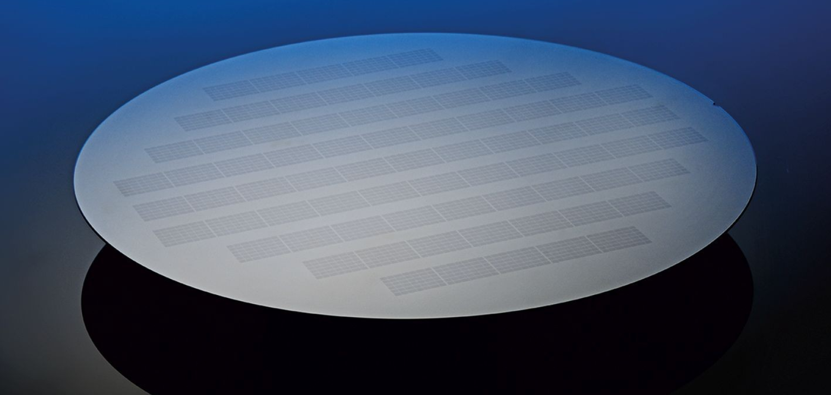
During manufacturing, MEMS sensor units are combined with an electronic, application-specific integrated circuit (ASIC) that sits on a silicon carrier unit (wafer).
This ASIC, which incorporates temperature-sensitive CMOS transistors, may not exceed 450°C during manufacturing. It is for this reason that the MEMS sensors, which are often made using crystalline silicon, are first manufactured separately – using high-temperature processes – and are later contacted with the ASIC via wire and solder connections or wafer bonding processes.
However, this conventional interconnection technology “requires a relatively large amount of space and prevents further miniaturisation of the MEMS and enhancement of their performance,” explained Florian Fuchs, a research associate in the Thin Film Processing group at Fraunhofer ILT.
Therefore, as an alternative to conventional joining techniques, Fraunhofer ILT has been developing a selective laser-based crystallisation process that, when combined with a silicon layer deposition process – developed by sister institutes Fraunhofer IST and ISIT – enables crystalline silicon MEMS sensors to be built directly (monolithically) on temperature-sensitive ASICs.
The collaborative work takes advantage of the fact that amorphous silicon layers can be produced at high deposition rates on the wafer holding the circuit at temperatures below 450°C. The laser then not only crystallises this silicon layer, but also activates the dopants it contains, thus ensuring suitable electrical conductivity. Subsequently, the sensor units are processed further using classic microelectronic manufacturing processes.
The crystallisation laser has a beam diameter of a few 10µm and is guided by a mirror to scan the entire surface step by step. The silicon is crystallised at high-temperature, but below its melting point, enabling crystallisation to occur spatially, selectively and very quickly (in the lower millisecond range). This way – in conjunction with targeted temperature management – the process minimises mechanical stresses in the layer material, but does not damage the sensitive electronics on the underlying substrate.
“Since the energy is quickly introduced into only a small volume, we achieve solid phase crystallisation of the silicon with laser processing at temperatures that are actually above the destruction threshold of the underlying circuit,” confirmed Dr Christian Vedder, head of the Thin Film Processing group at Fraunhofer ILT. “Due to the short local processing time, the circuit is nevertheless not damaged.”
The newly developed process reduces the electrical resistances of the silicon layers by more than four orders of magnitude, down to below a value of 0.05Ω*cm. At a layer thickness of 10µm, this value corresponds to a sheet resistance of 50Ω/sq. MEMS sensors with typical finger structures for a capacitive acceleration sensor could be produced from these layers.
New possibilities
“As crystalline silicon layers can be produced under CMOS-compatible conditions on an ASIC wafer, we are opening up new possibilities for integrating MEMS integrated circuits because it is no longer necessary to modify the CMOS manufacturing processes,” said Fuchs.
Since the process constraints have been eliminated, MEMS and integrated circuits can be developed independently, thus reducing development time and costs significantly. In addition to increasing integration density, the process eliminates wire connections and bond pads, thus leading to expected lower parasitic interference variables and improved shielding against electromagnetic interference fields. This elimination, in turn, has a positive effect on the signal quality and drift behaviour of the sensors.
The knowledge gained throughout the collaboration can be broadened and developed in several directions, according to the partners. For example, the process could be adapted to the specific requirements of different sensor types with different layer thicknesses or other doping materials. Fuchs elaborated: “We are now looking for users from industry who can profitably use the process our team has developed for their products.”
The prospect of increased performance combined with miniaturisation also makes MEMS technology attractive for other fields of application whose requirements cannot yet be met by today's MEMS systems. One conceivable application would be in the field of autonomous driving, where very precise acceleration sensors could bridge the gaps in GPS signal reception in tunnels or parking garages. The process also offers interesting potential in medical technology, for example, to integrate temperature sensors into headphones and use the data obtained to monitor patients or to fight pandemics. In addition, miniaturised, high-precision acceleration MEMS sensors could help precisely locate firefighters in burning buildings and thus increase the safety of emergency personnel.
