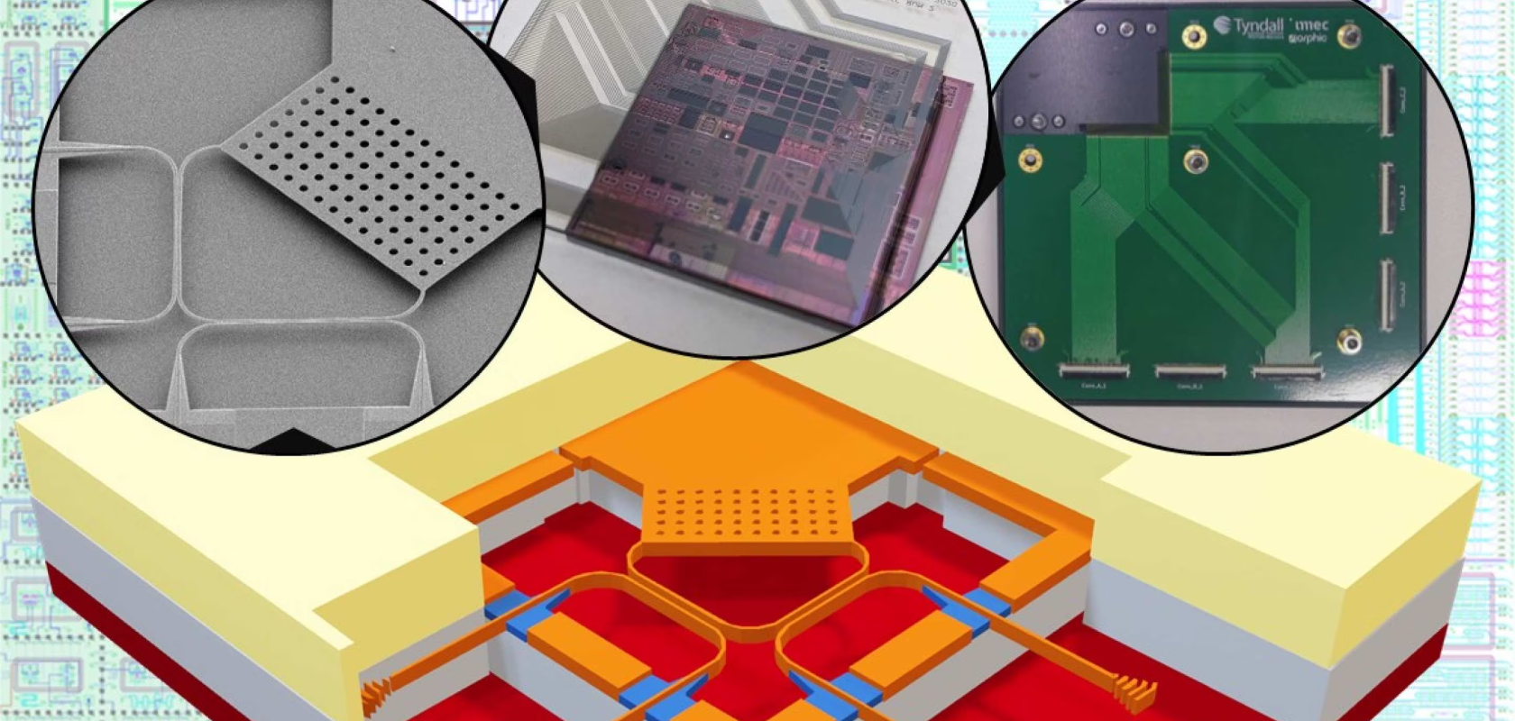
Scientists from the University of Sydney have developed a new microfabrication process that combines optics and micro-electro mechanical systems (MEMS) on a silicon microchip platform.
Described in Nature: Microsystems and NanoEngineering, the new process builds on silicon photonics and uses semiconductor manufacturing techniques.
It could enable the more energy-efficient generation of devices for fibre-optical telecommunications, future quantum computers, micro-3D cameras and gas sensors.
Associate Professor Quack, from the University’s School of Aerospace, Mechanical and Mechatronic Engineering, said that the photonic MEMS are unique in that they are fast, compact, consume very little power, support a broad range of optical carrier signals and have low optical loss.
“This is the first time that nano-electro-mechanical actuators have been integrated in a standard silicon photonics technology platform,” he said. “It is an important step towards mature large-scale, reliable photonic circuits with integrated MEMS. This technology is being prepared for high-volume production, with potential applications in 3D imaging for autonomous vehicles or new photonic assisted computing.”
According to Quack, current similar technologies consume a lot of power and occupy a large area on-chip. They also have high optical losses, which makes the integration of a large number of components on a single chip challenging.
“Our silicon photonic MEMS technology overcomes these shortcomings, providing a route for efficient scaling of photonic integrated circuits,” he said. “The technology will advance knowledge in the field of micro- and nanofabrication, photonics and semiconductors, with a wide range of applications. These include beam steering for lidar 3D sensing in autonomous vehicles, programmable photonic chips, or information processing in quantum photonics.”