Scientists have designed a laser diode that emits what they say is the shortest-wavelength ultraviolet (UV) light achieved to-date, with potential applications in disinfection, dermatology, and DNA and gas analysis.
In Applied Physics Express, the researchers, from Nagoya University in Japan, in partnership with Asahi Kasei Corporation, described how their deep-UV laser diode overcomes several issues encountered by scientists when working towards the development of such semiconducting devices, which have previously only been able to achieve emissions down to 336nm.
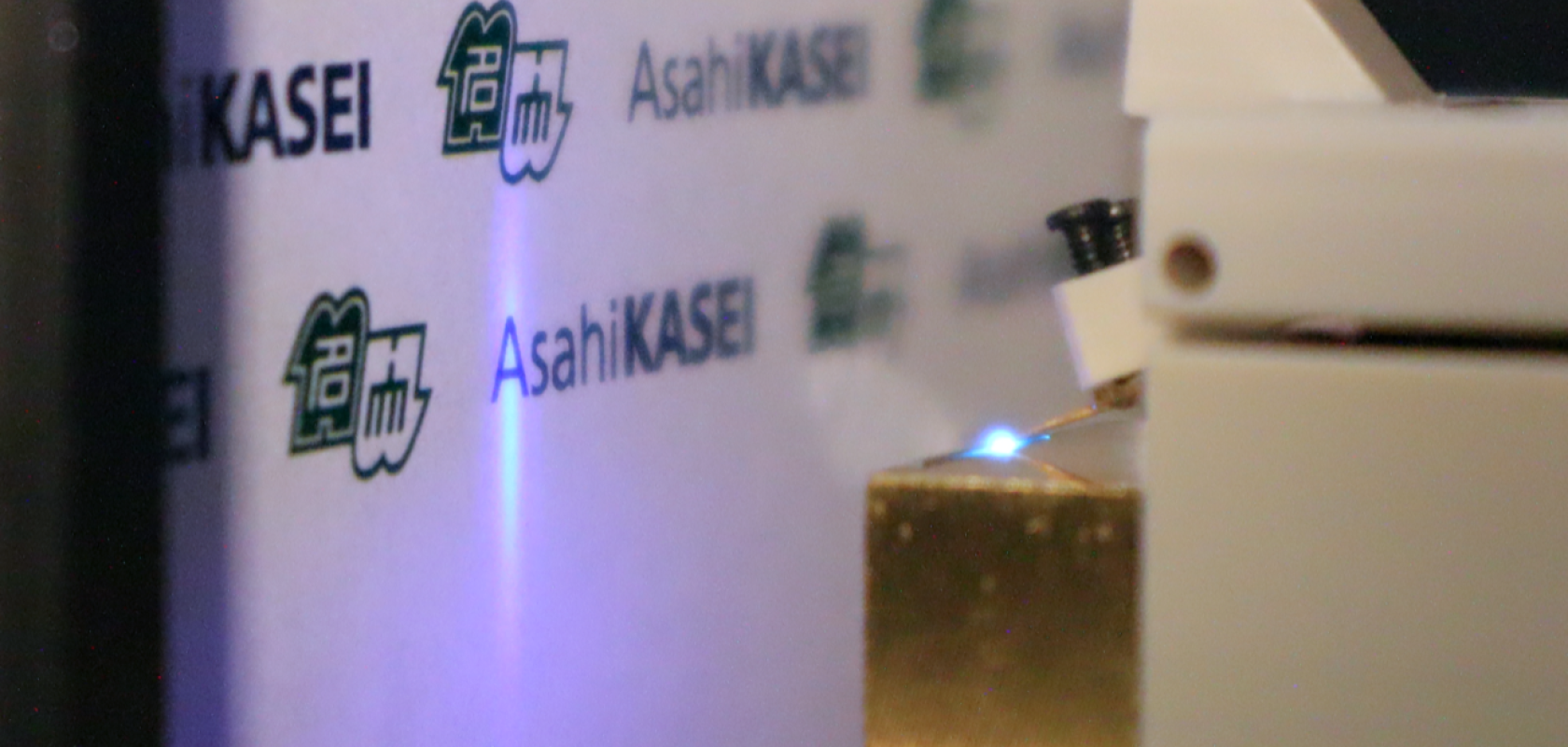
'Our laser diode emits the world's shortest lasing wavelength, at 271.8nm, under pulsed [electric] current injection at room temperature,' said Professor Chiaki Sasaoka of Nagoya University's Center for Integrated Research of Future Electronics.
Laser diodes that emit short-wavelength UV – also known as UV-C, the wavelength region of 200 to 280nm – could be used for disinfection in healthcare, for treating skin conditions such as psoriasis, and for analysing gases and DNA.
The team describe how they have used a high-quality aluminium nitride (AlN) substrate as their base for building up the layers of the laser diode. This, they say, is necessary, since lower quality AlN contains a large number of defects, which ultimately impact the efficiency of a laser diode's active layer in converting electrical into light energy.
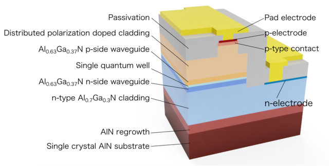
Figure 1: Cross-sectional structure of the UV-C semiconductor laser diode (Image: Asahi Kasei Corp. and Nagoya University )
In laser diodes, a 'p-type' and 'n-type' layer are separated by a 'quantum well'. When an electric current is passed through a laser diode, positively charged holes in the p-type layer and negatively charged electrons in the n-type layer flow towards the centre to combine, releasing energy in the form photons.
The researchers designed the quantum well so that it would emit deep UV light. The p- and n-type layers were made from aluminium gallium nitride (AlGaN). Cladding layers, also made from AlGaN, were placed on either side of the p- and n-type layers. The cladding below the n-type layer included silicon impurities, a process called doping. Doping is used as a technique to modify a material's properties. The cladding above the p-type layer underwent distributed polarisation doping, which dopes the layer without adding impurities. The aluminium content in the p-side cladding was designed so that it was highest at the bottom, decreasing towards the top. The researchers believe this aluminium gradient enhances the flow of positively charged holes. A top contact layer was finally added that was made from p-type AlGaN doped with magnesium.
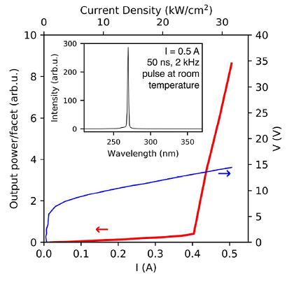
Figure 2: Emission characteristics under pulsed operation (Image: Asahi Kasei Corp. and Nagoya University)
The team found that the polarisation doping of the p-side cladding layer meant that a pulsed electric current of ‘remarkably low operating voltage’ of 13.8V was needed for the emission of ‘the shortest wavelength reported so far.’
Going forward the team will be conducting advanced joint research with Asahi Kasei Corporation to achieve continuous room temperature deep-UV lasing for the development of UV-C semiconductor laser products.
Their article can be read in Applied Physics Express here.
