Skip to main content
Social media links EO
LinkedIn
Twitter
Log in
Register
Applications
Life sciences
Environment
Quantum
Defence
Automotive
Aerospace
Medical engineering
Electronics
Optical communication
Technologies
Illumination & energy
Imaging
Industrial lasers
Lasers & optoelectronics
Sensors, test & measurement
Photonics 100
UK Photonics
Photonics Frontiers
Resources
Webcasts
White Papers
Supplier
Events
Products
Search
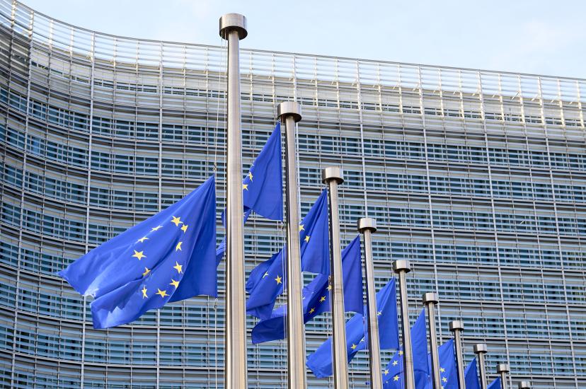
€288m support for European semiconductor supply chain approved by EU Commission
10,000-fold efficiency increase from Aalto’s million-cycle chip armour
Shilong Zhang wins 2026 SPIE Nick Cobb Scholarship for lithography research
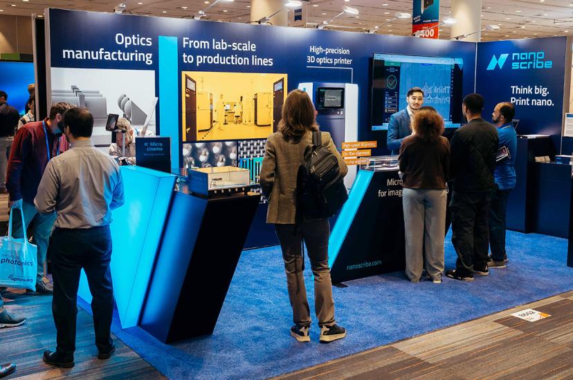
Nanoscribe demos scaled Quantum X system at Photonics West 2026
“Many AR capabilities are directly transferable to other domains, especially optical comms,” says Bernd Dielacher from EV Group
xLight secures $40m funding for EUV light source to improve semiconductor manufacturing
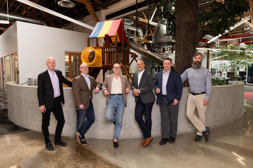
“We’ll build the world’s first quantum data centre”: Xanadu CEO on why the future of quantum is photonics
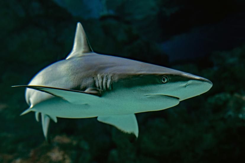
Shark skin surface to cut aircraft emissions with laser lithography manufactured coating
Growth in holographic lithography, SiPMs and optical sensors sees global photonics markets soar
Q&A: Hugo da Silva and Erhan Ercan from Morphotonics discuss the use of roll-to-plate technology for display innovations
Pagination
Page 1
Next page
››
Media Partners