After releasing a report on silicon photonics foundries, Iñigo Artundo, CEO of VLC Photonics, charts the evolution of the photonic foundry ecosystem
In the last few years there has been a resurgence in photonic integration technology. Photonic integration was proposed originally in the 1970s but only made its commercial debut in the late 1990s with silica planar lightwave circuit (PLC) passive components. Nowadays, several generic technology platforms are competing to serve many markets and applications. The main ones are silicon photonics and indium phosphide (InP), together with dielectric platforms like PLC and silicon nitride (SiN). While other III-V compounds, polymers and lithium niobate (LiNbO3) are also proposed, they remain niche platforms for specific components.
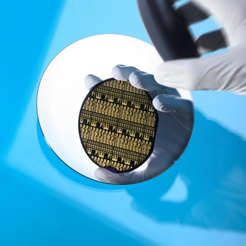
Focusing on silicon photonics, one of its main advantages is that it uses existing CMOS infrastructure, in terms of fab equipment and foundry facilities. Around a decade ago, pioneering European research institutions like Imec (Belgium), CEA Leti (France), IHP (Germany) and VTT (Finland) set up generic fabrication processes for silicon photonic circuits, including both dedicated and shared multi-project wafer (MPW) runs, where many users could share the available reticle area for prototyping their designs at a shared cost. Europractice, a service launched by the European Commission in 1995, started taking care of the brokerage of some of these silicon photonics MPW runs, and the ePIXfab consortium served as a European hub, promoting the technology and organising yearly training courses and many dissemination workshops. All these foundries now offer complete design manuals and process design kits (PDKs) to access their generic manufacturing processes, plus some customisation modules on the back-end too.
Outside of Europe, IME in Singapore has been providing similar silicon photonics foundry work, recently moving into commercial operation through the spin-off company AMF. In 2016, AIM Photonics emerged in the USA as an industry-driven public-private partnership, providing technology and services around photonic integration, including silicon photonics foundry services at the Suny Poly fab. Nowadays, the Mosis integrated circuit fabrication service is brokering for AIM Photonics processes.
Since then, many other commercial foundries have emerged to serve the booming data centre transceiver market. Several of them are well established CMOS foundries, like GlobalFoundries, TowerJazz or STMicroelectronics, and others like Compoundtek have emerged using third party process capabilities and their own photonic expertise.
Now, there are around 35 foundries offering different processes and services relating to silicon photonics, with each suited to different tasks: R&D prototyping, pilot production or volume mass manufacturing. These are distributed all over the globe, in Europe, USA and Asia, approximately one third for each region.
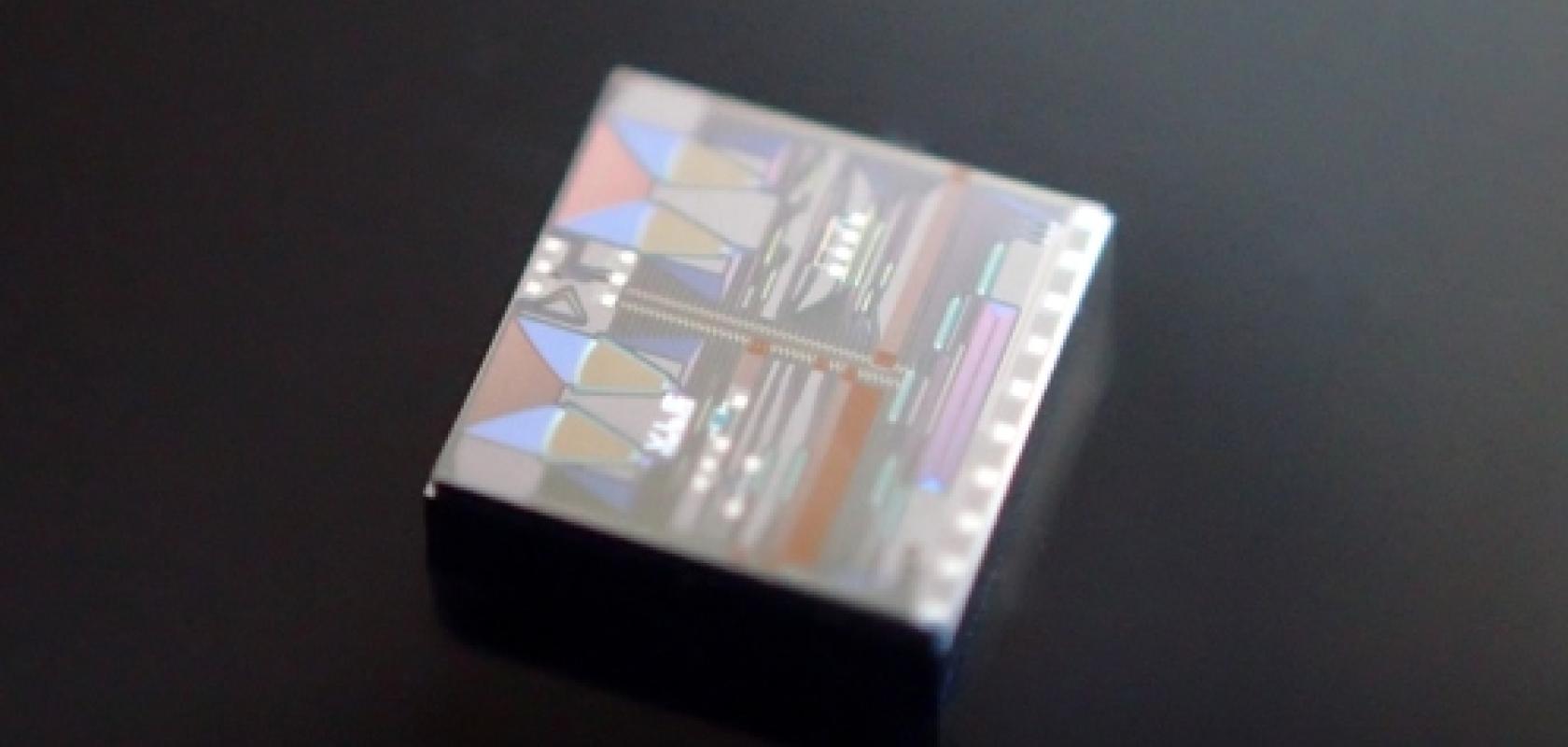
InP photonic integrated circuit with arrayed waveguide grating and other test structures, designed by VLC Photonics
There are fewer foundries available for InP. The two pioneers offering MPW runs are the R&D institute HHI in Germany, and the company Smart Photonics in The Netherlands. No other foundry offers shared runs at the moment, but many others do have processes that can be used to manufacture photonic integrated circuits (PICs). Similar to CMOS fabs, there are also RFIC fabs with InP HBT technologies that are now growing into photonics, like GCS in the USA.
However, given the more complex epitaxy design, growth and processing, foundries here tend to have custom processes rather than generic ones, many times adapted for specific customer’s needs. Hence, there are not as many MPW runs and, for custom runs, the scalability and yield can be sometimes worse than in silicon photonics. Nevertheless, InP remains one of the most widely used material platforms for integration given its intrinsic availability of light sources and amplifiers, making it a much more versatile platform in terms of functionality.
Finally, silicon nitride is also consolidating as one of the main material platforms. Even if it is mainly a passive platform, its low loss capabilities, its good fibre-to-chip coupling, and its possibility to operate in the visible wavelength range, are opening the door to many applications where it excels over the alternatives. The availability of periodic MPW runs at CNM (Spain), Ligentec (Switzerland) and LioniX International (The Netherlands) allows for a good transition from prototyping to production. It is worth mentioning here the European effort being made to develop a SiN pilot line, PIX4life, for fabricating photonic circuits at visible wavelengths. This started in 2016 and is now in the early open-access phase. Moreover, many silicon photonics foundries are also incorporating SiN layers into their processes as an option nowadays.
In summary, there has been a bloom of photonic foundry services in the last decade, with the few mentioned above as some of the most prominent and mature examples. Market demand is growing, and it is yet to be seen if the processes and PDKs will mature at an adequate pace to follow demand.
--
VLC Photonics’ silicon photonics foundry report details 35 international foundries and six foundry brokers operating in silicon photonics. It provides analysis of the different foundries' capabilities, facilities, equipment, processes, component libraries, and previous and on-going work.
VLC Photonics provides solutions for integrated optics: consultancy and engineering studies, in-house optical chip design, characterisation and test, and complete prototyping through external manufacturing and packaging/assembly partners. The fabless design house assists companies and researchers in their photonic integration projects, and collaborates with a wide network of foundries in all main material platforms. The report is available at www.vlcphotonics.com.