Dr Jose Pozo, director of technology and innovation, European Photonics Industry Consoritum (EPIC), discusses the association's recent trip to Japan, which focused on PIC technology
While the majority of EPIC events are held in Europe, technology and business have no borders, so we strive to connect our members with leaders and experts from the international photonics community. This year, delegation trips have been organised to Israel, Singapore, China and Japan. In addition, events are held annually at OFC and Photonics West in the USA.
From 7 to 10 November in Tokyo, EPIC brought together various industrial actors in photonic integrated circuits (PICs), and arranged a company visit to Hamamatsu Photonics. The size of the group was perfect for networking, and well-balanced for a global event (15 Europeans, 5 Canada/USA and 31 Japanese).
The main market for the Japanese companies remains datacom-telecom, evidenced by the presentations by Fujikura, the National Institute of Advanced Industrial Science and Technology (AIST) and Fujitsu, while in Europe newer markets such as medical imaging, biosensors, lidar, microwave photonics and even quantum are predominant.
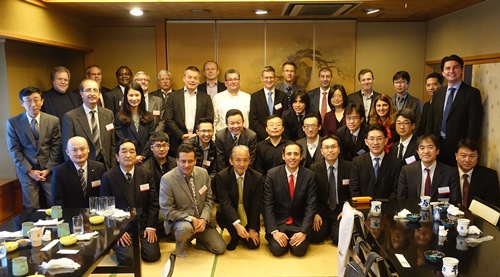
51 experts in photonics integrated circuits gather in Tokyo
A presentation by NTT Microsystem Integration Laboratories on the integration of silicon photonics and III-V materials by means of membrane technology was one of the highlights of the event. Imec in Belgium has also done extensive research on this topic, and their collaboration with TU Eindhoven on silicon photonics integration was mentioned as the European counterpart. As platforms for low losses, the thick silicon platform developed by the VTT Technical Research Centre of Finland was presented, as well as the TripleX platforms and their benefits for imaging and sensing.
The integration of PICs and electronics on chip, such as the BiCMOS integration proposed by the German Innovations for High Performance Microelectronics (IHP) institute, could solve some of the problems raised by companies in Japan, such as Fujitsu and Kyocera, which are proposing a 2.5D integration approach. The H2020 PETRA (Photonic Environment moniToring and Risk Assessment) project has developed a FPGA for the integration of electronics on PIC, also using a 2.5D approach. InP PIC platforms of Smart Photonics and Fraunhofer HHI were considered of high relevance and a clear alternative to hybrid integration of silicon photonics.
Packaging and testing are still two major bottlenecks in PIC technology. FiconTec and AifoTec showed their important role in the value chain as equipment manufacturer for both the packaging and testing. Physik Instrumente (PI) and OFS showed how the tools for such automation are as important as the equipment itself.
Pixapp was presented as the European pilot line for the manufacturing of PICs. On the testing side, Yenista showed how to test at wafer level and Yelo at device level. One of the conclusions was that polymer photonics is a more popular solution as a PIC platform in Japan than in Europe, as was evidenced by the presentation by Sumitomo. New parts of the value chain such as the materials provided for silicon photonics by Nissan Chemical Industries, showing the Sunconnect polymer for waveguide fabrication. Europe is clearly a very strong player in the field of photonic integrated circuits!