Stéphanie Le Calvez, head of architectures for the Photonic System Lab at CEA-Leti, discusses her group’s work in ensuring the AR experience lives up to its promise
Displays are part of our everyday lives, from TV sets to computers and smartphones. But while they help make our lives easier and more connected than ever, they don’t deliver the highly immersive experience, the enhanced-communication experience promised by augmented reality (AR).
Smart glasses will be the next digital medium to enable highly immersive experiences. But current models don’t make us dream like they should. The technology behind them is limited: bulky glasses with low brightness and a narrow field of view just do not do the trick.
There are two primary challenges to overcoming this barrier and producing smart glasses that deliver the technology’s full potential. On the one hand, the scientific community developing these glasses typically uses commercial components to create the optical systems. On the other hand, the innovative components that this community does create for the glasses, are developed without any consideration of the full optical system, which seriously limits the components’ compatibility with those systems.
With these challenges in mind, CEA-Leti embraced a new approach that leverages disruptive systems to build innovative components that are compatible with, and easily integrated in, optical systems. This new dynamic creates a virtuous circle in which the system itself will also help to create innovative components.
To support AR system-related projects that include optical components, the institute created a dedicated Architectures of Photonic Systems Lab. The new lab, which merges CEA-Leti’s display lab and x-ray detector lab, gathers 30 experts backed by world-class, pre-industrial equipment and a 91,500ft2 (~27,900m2) cleanroom. The lab has developed three essential technologies to help companies commercialise smart glasses, or head-mounted displays (HMD): new emissive LED microdisplays, curved OLED CMOS microdisplays and retinal projection.
The bright side
All AR applications require extremely high brightness, considering both the very high luminosity losses in optical systems and the high level of luminosity required to display images during sunny days. Improving display brightness with microLED technology has therefore been a primary focus of CEA-Leti’s new lab. Tapping into their 10 years of R&D experience in displays and lighting, the lab experts developed a new type of emissive microdisplay that can supply hundreds of thousands of nits. A first process flow based on hybridisation technology produced an 853 x 500 pixels video display.
Pixelisation at 10µm pitch was achieved on a GaN material and then reported on CMOS with microtubes plugged onto soft pads on the GaN material. The microtubes ensure both mechanical connection and electrical contact. A second process flow, based on a monolithic fabrication approach, helped reach very small pitches – 3µm – with higher brightness. Currently, GaN arrays are available in monochrome. The lab’s next challenge is to achieve a full colour microLED display.
Make it curved!
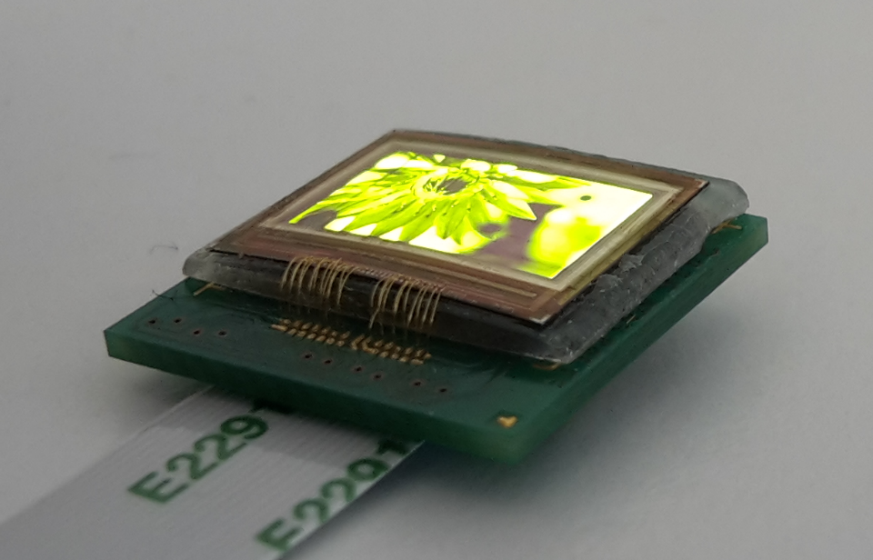
Figure one: WVGA OLED convex displays curved with 45mm radius, as specified in the LOMID European project
To reduce the size of the glasses, CEA-Leti developed and integrated a curved image sensor, called Pixcurve, which was demonstrated at CES 2019. The institute already demonstrated an impressive simplification of the optical system – 40 per cent fewer lenses required – and a 2.5x reduction of the total lens length compared to equivalent commercial systems. The team also identified a unique process flow to curve an OLED display at wafer-level scale with a 45mm radius of curvature. This technology consists of thinning the silicon wafer till it resembles a sheet of paper. The challenge in the case of OLED technology is that the OLED stack is done before the thinning of the wafer, and this water-sensitive layer needs to be protected all along this process – a world-first. The curvature can be either concave or convex. A preliminary ray-tracing study integrating a WVGA OLED microdisplay in an HMD optical system, shows that only four lenses are required, instead of five, making the system more compact and improving image quality.
Retinal projection
Combining integrated optics and holography is a new way to produce high-quality images for the scientific community developing display applications. This unconventional imaging concept helps lessen the impact of standard limitations of HMDs, by creating and transporting the image into the combiner. With this technology, the eye is the unique optical system and the image is formed directly on the retina. In this system, integrated photonics circuits transport light from the source to the eye as a data transfer system, and holography transforms this data into wavefronts for the image to be projected on the retina (see figure two below). The image is formed by leveraging visual-data transmission through a two-dimensional network of optical waveguides that addresses distribution of switchable holographic elements.
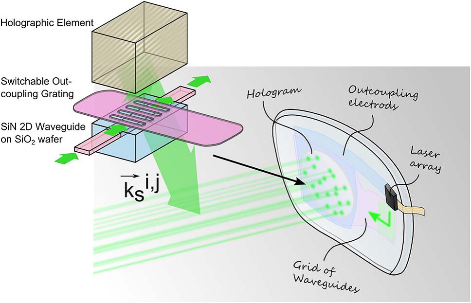
Figure two: artist’s view of the see-through display device with a zoom-in on one emissive point element
This optics-and-holography technology helps produce see-through and compact glasses.
Studies are underway to demonstrate three main features of this retinal-projection concept in which images are formed by a self-focusing effect, waveguide distribution arrays help address the right group of holographic elements to light on, and the directional holographic elements generate the wavefront.
In short, CEA-Leti is pursuing several pathways to address augmented reality’s new field of research by finding the way to adapt or to create new components. These include: developing high brightness video GaN micro displays with a pitch lower than 3µm; developing curved OLED CMOS microdisplays with a unique process that includes reliable encapsulation; packaging to protect components along the technological steps; and using a waveguide array associated to pixellated holograms to address augmented reality. EO