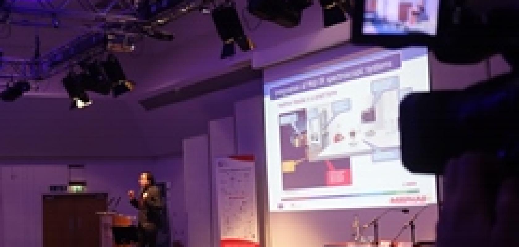
Steve Riches from the International Microelectronics, Assembly and Packaging Society (IMAPS UK), reports from November's Photonics and Opto-Electronics Packaging (POP) conference, which took place on 22 and 23 November in Edinburgh
The growing demand for silicon photonics, driven by the exponential expansion in data centre traffic, is posing challenges for opto-electronic packaging techniques in order to increase transmission rates and reduce manufacturing costs. The burgeoning opto-electronics industry is responding through moving to wafer scale packaging and collaboration through the establishment of pilot lines to reduce entry costs for photonic integrated circuits, said Peter O’Brien of Tyndall National Institute, Ireland, during his keynote speech at the Photonics and Opto-Electronics Packaging (POP) conference, which took place from 22 to 23 November in Edinburgh.
This jointly organised IMAPS-UK/EPIC/SEMI/JEMI summit, hosted by the Centre for Innovative Manufacturing in Laser-Based Production Processes at Heriot Watt University, was attended by leading players from industry and research in photonics packaging. The conference covered a range of topics, including user perspectives, packaging design/software, packaging services/equipment/testing and integrators/case studies in telecommunications, data centre and sensing sectors.
O’Brien, head of photonics packaging research at the Tyndall National Institute, plotted the growth of the monolithic photonic integrated circuit (PIC) and highlighted that the current assembly, test and packaging costs accounted for up 80 per cent of the overall unit costs. The need to reduce overall costs has led to research into the adoption of wafer scale packaging processes, with the added complications of integrating micro-optics, electronic components and thermal management.
The forecast market for silicon photonics was described by Eric Mounier from Yole Développement, France, who noted that an exponential growth in data centre traffic will fuel a boost in the need for photonic integrated circuits. Silicon photonics will be most attractive in 500m to 2km segments, where there will be an acceleration in the need for 400Gb/s transceivers instead of the 100Gb/s that are becoming available on the market in 2016.
The market prediction for transceivers is $6 billion by 2025, with a market value at chip level of $1.4 billion. Other applications will include environmental sensors, bio-sensors and lidar. There will be increasing pressure to reduce packaging costs towards a target of $1/Gb through wafer scale processing and increasing automation.
The packaging challenges are being tackled through a variety of approaches, such as improving the performance and efficiency of silicon photonic modules; developing automated assembly and test equipment with high accuracies; creating generic packaging platforms to standardise designs; and establishing open access facilities across Europe to enable low cost entry into manufacturing of photonic products.
Improved performance and efficiency of photonic devices
The main issues concerning device yield and reliability, electrical and optical packaging and thermal management were described by Nicola Pavaretti of Huawei Technologies, a company focusing on reducing packaging costs through automated assembly and testing. High accuracy assembly and low insertion loss optical coupling were identified as key areas. Karl Otto Velthaus of Fraunhofer HHI explained that a key parameter to control in high speed transceiver design is the impedance, and provided a perfectly controlled and matched impedance can be achieved enhancements in performance can be obtained.
Antonio La Porta of IBM Research demonstrated the performance enhancements achievable with polymer waveguides and their interfacing with the silicon photonics devices, while Ramsay Selim of Kaiam described the assembly of 100Gb/s and higher transceivers based on a silicon MEMS breadboard, which includes active alignment and fixing of optical components. Michael Robertson of Huawei-CIP discussed low cost packaging solutions in PICs with large port counts through a transfer printing method.
Photonics in high reliability and harsh environment applications was also covered by Dmitrij Siskin of Oxsensis, where optical sensor heads had been developed for gas turbine applications operating at temperatures of up to 1,200°C and Mikko Karpinnen of VTT demonstrated high performance optical interconnects for aerospace and space applications based on LTCC (low temperature co-fired ceramic) technology. Alessio Corazzo of SAES Group described the need to remove sulphur and halogen based compounds, moisture and volatile organic compounds (VOCs) due to their deleterious effects on LED device performance in sealed or semi-sealed environments using getters.
High accuracy automated assembly and test equipment
Ignazio Piacentini of FiconTEC saw the key to solving the packaging cost issue through automated equipment, adapted specifically for photonics assembly requirements, including 6 DOF motion equipment with sub-micron accuracies and machine vision. Guenael Ribette of Microtest introduced a high accuracy flexible bonding machine for research, development and low volume production. Martin van Acht of MA3 Solutions has developed a method for assembling a fibre array with accuracies of ±1µm, capable of handling >1,000 fibres on 250µm pitch, using mechanical fixing on an automated pick-and-place machine.
Generic packaging platforms
Several packaging suppliers are creating generic packaging platforms to ease the entry costs into photonics products, including a 'FotonIC' platform containing standardised optical and electrical I/Os as described by Andrew Thompson of Optocap, a silicon photonics and InP platform for high end components and sub-systems operating between 10 and 100Gb/s in low to medium volumes presented by Antonello Vannucci of Linkra and an integrated photonics platform that is scalable to volume production by Joost van Kerkhof of Lionix International.
Open access facilities for photonics manufacturing
In order to bridge the gap between photonics design and achieving volume manufacturing, there are several ongoing initiatives in Europe to stimulate manufacturing of photonics ranging from design assistance to establishing pilot production capabilities. Design assistance is available within the PICs4All project, where companies interested in developing PICs can access free advice on technical and economic viability, assistance on the design of PICs and guidance in access to manufacturing and packaging services, as described by Adrian Wonfor of the University of Cambridge. Hossein Moeini of Phoenix BV presented an introduction to Assembly Design Kits (ADKs) for photonic packaging, where a library of validated design and assembly building blocks are available to reduce design times for photonics packaging applications. Ewit Roos of Photon Delta described an initiative in The Netherlands, which brings together a complete value chain for photonics innovation, while Pim Kat said that Technobis Group are expanding their assembly facilities to cope with an expected increase in demand for PIC packaging.
Jose Pozo of MIRPHAB explained that a pilot production line is being established to design and manufacture sensors in the 3-12µm wavelength for gas detection, bio-sensing, spectrometry and other applications, and O’Brien of Tyndall Institute described the PIXAPP programme, where a distributed pilot packaging line for the design, manufacture and test of photonic circuits is being created. Andy Sellars, Lead Technologist at Innovate UK, described the plans for a Compound Semiconductor Applications Catapult Centre to tackle industry challenges for high energy densities and precision assembly in photonics, sensing, RF/microwave and power electronics as an open access facility.
The attendees also had the chance to meet leading industry supply chain members who provided a worthwhile exhibition of equipment, materials and solutions, to enable delegates to network during the refreshment breaks and find new sources of supply. In all this inaugural conference was very well received and it is hoped that many of the developments discussed will be forthcoming and made available for a repeat event next year.
For further information, please visit IMAPS-UK, EPIC, JEMI and SEMI.
Related stories
