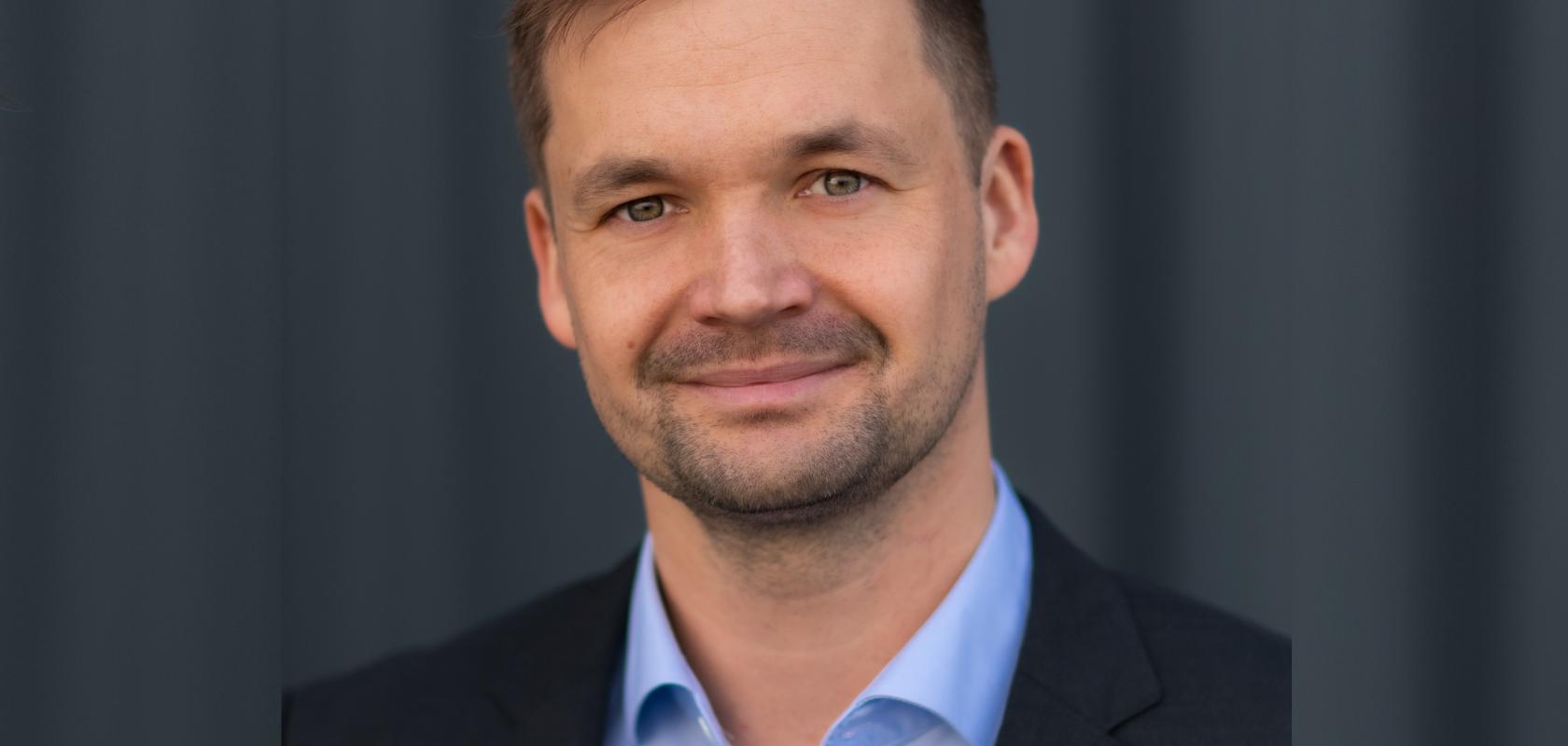
What’s the background to your appointment as CTO at 3D AG?
After 17 years of academic research I was ready to experience new challenges in the corporate world. When I found an interdisciplinary opportunity at 3DAG, I knew it was the right match.
A key pillar for my development had been my colleagues. It is thanks to the support of the team that I could successfully implement new ideas, processes, and technologies.
When shown trust, one builds the confidence and space to grow, and that is what 3D AG’s CEO, Martina Muller, has given me since the start.
It all started in 2005 in Wroclaw, my hometown in Poland, where I studied an MSc in Engineering & Biomedical Optics at Wroclaw University of Science and Technology. In my final year, I did an internship for my master’s thesis at Philips Research in Eindhoven, The Netherlands, where I worked on characterising light scattering structures. During these years, my passion for research began and, by 2010, I successfully applied for a research assistant position at Empa (the Swiss Federal Laboratories for Materials Science and Technology).
Those years were full of insightful knowledge and opportunities. I was working in the medical textiles groups and got the opportunity to develop technology around sensing solutions for blood oxygenation, glucose, and others. My curiosity and motivation must have given a good impression, since I was offered to continue my research work within a doctoral program at ETH Zurich. Over the next three years, my time was divided between the university and my research at Empa.
Upon finishing my doctoral dissertation, I moved to Lucerne University of Applied Sciences and Arts as a senior research associate working on light redirection systems in occupational buildings. Even though the work I was performing was very interesting, I realised I was ready for the next big thing. I felt that, after almost 12 years of dedicating my life to academia, I needed new perspectives and experiences.
I could say we found each other at the right time – 3D AG was looking for an engineer with an interdisciplinary background, and I was looking to apply my knowledge to a corporate environment. My colleagues appreciated that I was not shy to speak up and suggest improvements!
After two years, I was promoted to Director of Technologies and R&D with responsibility for managing a small team in the design and implementation of custom processes. And in September 2022, I was appointed 3D AG’s CTO.
What does 3D AG do and what are your main markets?
We are a small, family-owned company, with an extensive global reach. We were founded in 1989 as a high-security company for the origination and mastering and production of holographic features. We have a worldwide portfolio of customers, and our main markets are split equally between high security (e.g. identity, banknotes and precious metals), brand protection (e.g. anti-counterfeiting, digitalisation opportunities and licensing merchandising), and functional structures, which are used in various applications such as tooling for injection moulding, solar cells, LCD displays and anti-reflective surfaces.
We work with interferometric processes whereby a laser beam is split to produce a holographic image on a glass plate. Later, the glass plate with the nanostructure will be turned into a tool for mass production, which is done by high-precision nickel electroforming to give an exact copy down to the nanometre level of the master structure.
Over the years, we’ve also grown towards the development of microfluidic functional structures with electroforming processes and producing tools for embossing or the production of microfluidic chips.
What were your main challenges when you first came to 3D AG?
The learning curve I went through when starting in the company was, perhaps, the biggest challenge for me. The first six months was an intensive learning period, particularly regarding the chemistry behind electroforming and UV-curable resin.
How do you see the future?
The future looks bright for us, with plenty of new challenges and working processes to adapt. One of our priorities is to split our R&D into internal and external for customers. This will allow us to better visualise our priorities and place clear objectives.
As regards to the markets, we will continue directing our attention to high-security and functional applications, which are both getting tighter and more competitive.
We are aware that the accuracies for positioning and other kinds of tolerances are becoming increasingly tighter. We’ve just built a new machine that took three years of R&D with the engineering office to develop. This has improved our machine accuracies by a factor of 10, but it’s a never-ending story.
In relation to the competition, while there are many companies doing electroforming for microstructures, most are doing it as in-house processes. Our advantage is that we deliver our products to external partners.
What problems do you have in recruiting and retaining talent?
We are a company with about 20 employees and our policy has always been around sustainable growth, rather than looking for millions in investment to fund rapid growth. Over the past two years, we have needed to recruit five people, of which one is a research engineer and the other a technician.
Recruitment and retention of talent are never easy, but our advantage is we are an interesting and attractive company. We are small, so we all know each other. We work with a variety of processes… you would only expect to find this diversity in a multinational!
If you started again, what would you do differently?
I don’t have the habit of looking back and wanting to change my decisions – I would rather be happy with myself and my development over the years. It’s normal to have small setbacks that one does not expect every now and then. What’s important is not to focus on the mistakes, but learn from them and move on to the next chapter.


